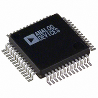
ADV7197KSZ Analog Devices Inc, ADV7197KSZ Datasheet - Page 9

ADV7197KSZ
Manufacturer Part Number
ADV7197KSZ
Description
IC DAC VID-HDTV 3CH-11BIT 52MQFP
Manufacturer
Analog Devices Inc
Type
Video Encoderr
Datasheet
1.ADV7197KS.pdf
(20 pages)
Specifications of ADV7197KSZ
Applications
HDTV
Voltage - Supply, Analog
3.15 V ~ 3.45 V
Mounting Type
Surface Mount
Package / Case
52-MQFP, 52-PQFP
Adc/dac Resolution
11b
Screening Level
Industrial
Package Type
MQFP
Pin Count
52
Lead Free Status / RoHS Status
Lead free / RoHS Compliant
Voltage - Supply, Digital
-
Lead Free Status / RoHS Status
Compliant, Lead free / RoHS Compliant
Pin
1, 12
2–11
13, 52
14–23
24, 35
25
26, 33
27
28
29
30
31
32
34
36
37
38
39
40
41
42–51
Mnemonic
V
Y0–Y9
GND
Cr0–Cr9
V
CLKIN
AGND
DV
VSYNC/
TSYNC
HSYNC/
SYNC
SCL
SDA
DAC C
DAC A
DAC B
COMP
R
V
RESET
ALSB
Cb/Cr9–0
DD
AA
SET
REF
Input/Output
P
I
G
I
P
I
G
I
I
I
I
I/O
O
O
O
O
I
I/O
I
I
I
PIN FUNCTION DESCRIPTIONS
Function
Digital Power Supply.
10-Bit HDTV Input Port for Y Data. G data input in RGB mode.
Digital Ground
10-Bit HDTV Input Port for Color Data in 4:4:4 Input Mode. In 4:2:2 mode this
input port is not used. R data input in RGB mode.
Analog Power Supply.
Pixel Clock Input. Requires a 74.25 MHz (74.1758 MHz) reference clock.
Analog Ground
Video Blanking Control Signal Input.
VSYNC, vertical sync control signal input or TSYNC input control signal in
Async Timing Mode.
HSYNC, horizontal
Async Timing Mode.
MPU Port Serial Interface Clock Input.
MPU Port Serial Data Input/Output.
Color component analog output of input data on Cb/Cr9–0 input pins.
Y Analog Output.
Color component analog output of input data on Cr9–Cr0 input pins.
Compensation Pin for DACs. Connect 0.1 µF Capacitor from COMP pin to V
A 2470 Ω resistor (for input ranges 64–940 and 64–960, output standards
EIA-770.3) must be connected from this pin to ground and is used to control the
amplitudes of the DAC outputs. For input ranges 0–1023 (output standards
RS-170, RS-343A) the R
Optional External Voltage Reference Input for DACs or Voltage Reference
Output (1.235 V).
This input resets the on-chip timing generator and sets the ADV7197 into Default
Register setting. Reset is an active low signal.
TTL Address Input. This signal sets up the LSB of the MPU address. When this
pin is tied high, the I
When this pin is tied low, the input bandwidth on the I
10-Bit HDTV Input Port for Color Data. In 4:2:2 mode the multiplexed CrCb
data must be input on these pins. B data input in RGB mode.
2
C filter is activated which reduces noise on the I
sync control signal input or SYNC input control signal in
SET
value must be 2820 Ω.
2
C interface is increased.
ADV7197
2
C interface.
AA
.


