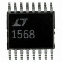
LT1568CGN#PBF Linear Technology, LT1568CGN#PBF Datasheet - Page 6

LT1568CGN#PBF
Manufacturer Part Number
LT1568CGN#PBF
Description
IC FILTER BUILDING BLOCK 16SSOP
Manufacturer
Linear Technology
Datasheet
1.LT1568CGNPBF.pdf
(16 pages)
Specifications of LT1568CGN#PBF
Filter Type
Bandpass
Frequency - Cutoff Or Center
200kHz
Number Of Filters
2
Max-order
2nd
Voltage - Supply
2.7 V ~ 11 V, ±2.7 V ~ 5.5 V
Mounting Type
Surface Mount
Package / Case
16-SSOP
Lead Free Status / RoHS Status
Lead free / RoHS Compliant
Available stocks
Company
Part Number
Manufacturer
Quantity
Price
FILTER ELECTRICAL CHARACTERISTICS
LT1568
Specifications are for the differential output (OUTA – OUTA or OUTB – OUTB) of a single 2nd order section (A or B), gain = –2,
R
which apply over the full operating temperature range, otherwise specifications and typical values are at T
V
SYMBOL
THD
Note 1: Absolute Maximum Ratings are those values beyond which the life
of the device may be impaired.
Note 2: The inputs of each op amp are protected by back-to-back diodes.
If either differential input voltage exceeds 1.4V, the input current should be
limited to less than 10mA.
Note 3: A heat sink may be required to keep the junction temperature
below the absolute maximum rating when the output is shorted
indefinitely.
Note 4: The inverter bandwidth is measured with the SA or SB output
floating, and is defined as the frequency at which the phase shift from
OUTA (OUTB) to OUTA (OUTB) drops from 180 to 135 .
Note 5: Measured with the SA or SB output connected in the filter
application circuit as shown in the Block Diagram.
Note 6: The common mode input voltage range is measured by shorting
the filter input to the common mode reference (GNDA or GNDB) and
applying a DC input voltage to search for the common mode voltage range
that creates a 2mV (V
or OUTB) voltage (measured with respect to GNDA or GNDB).
6
S
FIL
= single 5V, EN pin to logic “low,” R
= R11 = R21 = R31 = R12 = R22 = R32. All voltages are with respect to V
PARAMETER
Filter Gain Mismatch
Wideband Output Noise
Total Harmonic Distortion
(V
OUTA
– V
S
= 3V) or 5mV (V
OUTA
) – (V
OUTB
S
– V
= 5V) change in the (OUTA
LDIFF
OUTB
= 800 connected to midsupply, unless otherwise noted.
)
CONDITIONS
f
f
f
f
f
f
f
f
C
C
C
C
C
IN
C
IN
= 1MHz, f
= 10MHz, f
= 1MHz, R
= 10MHz, R
= 1MHz, R
= 10MHz, R
= 200kHz, V
= 2MHz, V
IN
FIL
FIL
IN
IN
FIL
FIL
= f
IN
= f
= 1V
= 1.28k, BW = 2MHz
= 1.28k,
C
= 128 , BW = 20MHz
= 128 ,
= 1V
C
P-P
Note 7: The minimum cutoff frequency of the LT1568 is arbitrarily listed
as 200kHz. The limit is arrived at by setting the maximum resistor value
limit at 6.4k. Due to input bias current, the output DC offset through a
single section can be as high as 25mV with resistors this large. The
LT1568 can be used with even larger resistors if the large offset voltages
can be tolerated. For cutoff frequencies below 200kHz, refer to the
LTC1563-2, LTC1563-3.
Note 8: With equal-sized resistors, the differential DC gain through either a
single section or cascaded sections is 6dB.
Note 9: The LT1568C is guaranteed to meet specified performance from
0 C to 70 C. The LT1568C is designed, characterized and expected to
meet specified performance from –40 C to 85 C but is not tested or QA
sampled at these temperatures. The LT1568I is guaranteed to meet
specified performance from –40 C to 85 C.
P-P
GND
= V
GNDA
= V
GNDB
. The
–0.3
–0.4
MIN
denotes the specifications
A
= 25 C.
TYP
– 84
– 69
0.10
0.15
36
88
MAX
0.3
0.4
UNITS
V
V
1568f
RMS
RMS
dB
dB
dB
dB


