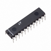
LTC1068CN#PBF Linear Technology, LTC1068CN#PBF Datasheet - Page 6

LTC1068CN#PBF
Manufacturer Part Number
LTC1068CN#PBF
Description
IC FILTR BUILDNG BLK QUAD 24-DIP
Manufacturer
Linear Technology
Datasheet
1.LTC1068CNPBF.pdf
(28 pages)
Specifications of LTC1068CN#PBF
Filter Type
Universal Switched Capacitor
Frequency - Cutoff Or Center
50kHz
Number Of Filters
4
Max-order
8th
Voltage - Supply
3.14 V ~ 11 V, ±3.14 V ~ 5.5 V
Mounting Type
Through Hole
Package / Case
24-DIP (0.300", 7.62mm)
Lead Free Status / RoHS Status
Lead free / RoHS Compliant
Available stocks
Company
Part Number
Manufacturer
Quantity
Price
LTC1068 Series
ELECTRICAL CHARACTERISTICS
apply over the full operating temperature range, otherwise specifications are at V
PARAMETER
DC Offset Voltage (Note 5)
(See Table 1)
Clock Feedthrough
Max Clock Frequency (Note 6)
Power Supply Current
Note 1: Stresses beyond those listed under Absolute Maximum Ratings
may cause permanent damage to the device. Exposure to any Absolute
Maximum Rating condition for extended periods may affect device
reliability and lifetime.
Note 2: Production testing for single 3.14V supply is achieved by using
the equivalent dual supplies of ±1.57V.
Note 3: Production testing for single 4.75V supply is achieved by
using the equivalent dual supplies of ±2.375V.
Table 1. Output DC Offsets One 2nd Order Section
TYPICAL PERFORMANCE CHARACTERISTICS
6
50
45
40
35
30
25
20
15
10
MODE
5
0
1b
1
2
3
0
LTC1068
Maximum Q vs Center Frequency
(Modes 1, 1b, 2)
10
CENTER FREQUENCY, f
A
V
V
V
[V
[R4/(R2 + R4)] + V
V
A. V
B. V
C. V
(FOR MODE 2 R4 ≥ 10R2)
20
OSN
OS1
OS1
OS2
OS1
S
S
S
[(1/Q) + 1 + ||HOLP||] – V
[(1/Q) + 1 + R2/R1] – V
(1 + R2/R1 + R2/R3 + R2/R4) – V
= 3.3V, f
= 5V, f
= ± 5V, f
30
B
CLK(MAX)
40
CLK(MAX)
CLK(MAX)
O
50
(kHz)
OS2
= 3.4MHz
W
= 5.6MHz
= 1.5MHz
[R2/(R2 + R4)]
C
60
1068 G01
U
OS3
70
OS3
/Q
CONDITIONS
V
(DC Offset of Input Inverter)
V
(DC Offset of First Integrator)
V
(DC Offset of Second Integrator)
V
V
V
V
V
/Q
S
S
S
S
S
S
S
S
= ±5V, f
= ±5V, f
= ±5V, f
= ±5V, f
= ±5V, Q ≤ 1.6, Mode 1
= 3.14V, f
= 4.75V, f
= ±5V, f
OS3
50
45
40
35
30
25
20
15
10
5
0
(R2/R3)X
LTC1068
Maximum Q vs Center Frequency
(Modes 2, 3)
0
CLK
CLK
CLK
CLK
CLK
CLK
CLK
= 1MHz, V
= 1MHz, V
= 1MHz, V
= 1MHz
= 1MHz
= 1MHz (Note 2)
= 1MHz (Note 3)
10
CENTER FREQUENCY, f
LTC1068-25 (Complete Filter). The
A
A. V
B. V
C. V
(FOR MODE 2 R4 < 10R2)
20
OS1
OS2
OS3
S
S
S
V
V
V
V
V
OSBP
= 3.3V, f
= 5V, f
= ± 5V, f
OS3
OS3
OS3
OS3
30
Note 4: Pin 7 (AGND) is the internal analog ground of the device. For
single supply applications this pin should be bypassed with a 1µF
capacitor. The biasing voltage of AGND is set with an internal resistive
divider from Pin 8 to Pin 23 (see Block Diagram).
Note 5: Side D is guaranteed by design.
Note 6: See Typical Performance Characteristics.
B
CLK(MAX)
CLK(MAX)
CLK(MAX)
40
O
V
V
~(V
V
V
OSLP
OSN
OSN
OS1
(kHz)
= 3MHz
OSN
= 5MHz
= 1MHz
[1 + R4/R1 + R4/R2 + R4/R3] – V
50
– V
– V
S
C
– V
= ±5V, T
OS2
OS2
1068 G02
OS2
60
●
●
●
●
●
●
)(1 + R5/R6)
A
= 25°V, unless otherwise noted.
MIN
●
55
50
45
40
35
30
25
20
15
10
denotes the specifications which
5
0
0
LTC1068-200
Maximum Q vs Center Frequency
(Modes 1, 1b, 2)
4
A
CENTER FREQUENCY, f
TYP
0.25
5.6
3.5
6.5
9.5
– 2
– 5
8
0
A: V
B: V
C: V
OS2
12
S
S
S
(R4/R2) – V
B
= 3.3V, f
= 5V, f
= ± 5V, f
(FOR MODE 2, R4 ≥ 10R2)
16
C
CLK(MAX)
MAX
±15
±25
±40
CLK(MAX)
CLK(MAX)
11
15
8
20
O
OS3
(kHz)
24
= 3.2MHz
(R4/R3)
= 6.1MHz
= 1.2MHz
mV
UNITS
28
1068fb
1068 G03
MHz
RMS
mV
mV
mV
mA
mA
mA
32


