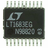
LTC1562CG-2#PBF Linear Technology, LTC1562CG-2#PBF Datasheet - Page 2

LTC1562CG-2#PBF
Manufacturer Part Number
LTC1562CG-2#PBF
Description
IC FILTER UNIV RC QUAD LN 20SSOP
Manufacturer
Linear Technology
Datasheet
1.LTC1562CG-2PBF.pdf
(16 pages)
Specifications of LTC1562CG-2#PBF
Filter Type
Universal, Continuous-Time
Frequency - Cutoff Or Center
300kHz
Number Of Filters
4
Max-order
8th
Voltage - Supply
4.75 V ~ 10.5 V, ±4.75 V ~ 5.25 V
Mounting Type
Surface Mount
Package / Case
20-SSOP
Lead Free Status / RoHS Status
Lead free / RoHS Compliant
Available stocks
Company
Part Number
Manufacturer
Quantity
Price
ABSOLUTE AXI U RATI GS
(Note 1)
Total Supply Voltage (V
Maximum Input Voltage
Storage Temperature Range ................. – 65 C to 150 C
Operating Temperature Range
Lead Temperature (Soldering, 10 sec).................. 300 C
LTC1562-2
ELECTRICAL CHARACTERISTICS
range, otherwise specifications are at T
specs are for a single 2nd order section, R
SYMBOL
V
I
V
H
2
S
S
OS
L
at Any Pin ....................(V
LTC1562C-2 ............................................ 0 C to 70 C
LTC1562I-2 ........................................ – 40 C to 85 C
PARAMETER
Total Supply Voltage
Supply Current
Output Voltage Swing, V2 Outputs
Output Voltage Swing, V1 Outputs
DC Offset Magnitude, V2 Outputs
DC AGND Reference Point
Center Frequency (f
Lowpass Passband Gain at V2 Output
Q Accuracy
Wideband Output Noise
Input-Referred Noise, Gain = 100
W
+
O
) Error (Notes 2, 3)
to V
W W
–
–
– 0.3V) V (V
) .............................. 11V
A
= 25 C. V
IN
= R2 = 10.4k 0.1%, R
CONDITIONS
V
V
V
V
V
V
V
V
V
V
V
V
V
V2 Output Has R
V
V
V
BW = 400kHz, f
S
S
S
S
S
S
S
S
S
S
S
S
S
S
S
S
U
S
= 2.375V, R
= 5V, R
= 2.375V, R
= 5V, R
= 2.375V, R
= 5V, R
= 2.375V, R
= 5V, R
= 2.375V, Input at AGND Voltage
= 5V, Input at AGND Voltage
= Single 5V Supply
= 5V, V2 Output Has R
= 2.375V, f
= 2.375V, V2 Output Has R
= 2.375V, BW = 400kHz, Input AC GND
= 5V, BW = 400kHz, Input AC GND
= 5V, outputs unloaded, SHDN pin to logic “low”, unless otherwise noted. AC
+
+ 0.3V)
The
L
L
L
L
= 5k, C
= 5k, C
= 5k, C
= 5k, C
O
IN
L
L
L
L
L
= 200kHz, Q = 1, Input AC GND
= 5k, C
= 5k, C
= 5k, C
= 5k, C
= 10kHz,
= 5k, C
denotes specifications that apply over the full operating temperature
L
L
L
L
Q
= 30pF, Outputs at 0V
= 30pF, Outputs at 0V
= 30pF
= 30pF, f = 250kHz
PACKAGE/ORDER I FOR ATIO
= 9.09k 0.1%, f
Consult LTC Marketing for parts specified with wider operating temperature ranges.
L
L
L
L
L
= 30pF, Outputs at 0V
= 30pF, Outputs at 0V
= 30pF
= 30pF, f = 250kHz
= 30pF
L
= 5k, C
SHDN
INV B
INV A
V1 B
V2 B
V2 A
V1 A
SUBSTRATE/SHIELD CONNECTIONS
*G PACKAGE PINS 4, 7, 14, 17 ARE
V
V
L
V
–*
–*
= 5k, C
+
T
AND MUST BE TIED TO V
JMAX
L
20-LEAD PLASTIC SSOP
10
1
2
3
4
5
6
7
8
9
= 30pF
= 150 C,
L
G PACKAGE
= 30pF
TOP VIEW
O
= 175kHz.
JA
= 136 C/W
20
19
18
17
16
15
14
13
12
11
–
INV C
V1 C
V2 C
V
V
AGND
V
V2 D
V1 D
INV D
–*
–
–*
U
4.75
MIN
4.2
9.3
8.4
0
+ 0.05
LTC1562CG-2
LTC1562IG-2
ORDER PART
22.5
TYP
4.6
9.8
4.5
9.7
2.5
0.5
7.3
+ 2
21
39
39
3
3
W
NUMBER
MAX
+ 0.1
10.5
23.5
1.7
25
28
30
17
17
UNITS
15622fa
U
V
V
V
V
V
V
V
RMS
RMS
RMS
mA
mA
mA
mA
mV
mV
P-P
P-P
P-P
P-P
dB
%
%
V
V


