MF10CCWM/NOPB National Semiconductor, MF10CCWM/NOPB Datasheet - Page 3
MF10CCWM/NOPB
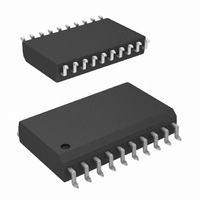
Manufacturer Part Number
MF10CCWM/NOPB
Description
IC FILTER DUAL SW CAP 20-SOIC
Manufacturer
National Semiconductor
Datasheet
1.MF10CCWMNOPB.pdf
(28 pages)
Specifications of MF10CCWM/NOPB
Filter Type
Universal Switched Capacitor
Frequency - Cutoff Or Center
200kHz
Number Of Filters
2
Max-order
4th
Voltage - Supply
±9 V ~ 14 V
Mounting Type
Surface Mount
Package / Case
20-SOIC (7.5mm Width)
Lead Free Status / RoHS Status
Lead free / RoHS Compliant
Other names
*MF10CCWM
*MF10CCWM/NOPB
MF10CCWM
*MF10CCWM/NOPB
MF10CCWM
Available stocks
Company
Part Number
Manufacturer
Quantity
Price
Company:

Part Number:
MF10CCWM/NOPB
Manufacturer:
AD
Quantity:
8 356


Symbol
V
V
V
V
GBW
SR
I
SC
Electrical Characteristics
OS3
OS2
OS3
OUT
V
25˚C.
Logic Input Characteristics
CMOS Clock
Input Voltage
TTL Clock
Input Voltage
+
Boldface limits apply for T
= +5.00V and V
(Note 5)
DC Offset Voltage
(Note 5)
DC Offset Voltage
(Note 5)
DC Offset Voltage
(Note 5)
Minimum Output
Voltage Swing
Op Amp Gain BW Product
Op Amp Slew Rate
Dynamic Range(Note 6)
Maximum Output Short
Circuit Current
(Note 7)
Parameter
−
= −5.00V unless otherwise specified. Boldface limits apply for T
Min Logical “1”
Max Logical “0”
Min Logical “1”
Max Logical “0”
Min Logical “1”
Max Logical “0”
Parameter
MIN
to T
MAX
; all other limits T
(Continued)
Max
Min
Max
Min
Max
BP, LP Pins
N/AP/HP
Pin
Source
Sink
V
V
V
V
V
V
+
LSh
+
LSh
+
LSh
= +5V, V
= +10V, V
= +5V, V
= 0V
= +5V
= 0V
Conditions
−
−
−
= −5V,
= −5V,
(f
50)
V
(f
50)
V
(f
50)
V
(f
100)
V
(f
100)
V
(f
100)
R
R
V
(f
V
(f
A
= 0V,
CLK
CLK
CLK
CLK
CLK
CLK
CLK
CLK
pin12
pin12
pin12
pin12
pin12
pin12
pin12
L
L
= T
= 5k
= 3.5k
3
/f
/f
/f
/f
/f
/f
/f
/f
O
O
O
O
O
O
O
O
J
= +5V
= +5V
= 0V
= 0V
= 0V
= +5V
= 0V
= 25˚C
=
=
=
=
=
=
= 50)
= 100)
Conditions
(Note 8)
Typical
S
All Modes
S
S
All Modes
A/B
A/B
A/B
= V
= V
= V
MF10ACN, MF10CCN,
−
+
−
MF10CCWM
MIN
(Note 9)
Tested
Typical
Limit
+3.0
−3.0
+8.0
+2.0
+2.0
+0.8
to T
±
±
(Note
−300
−140
−140
−70
−70
2.5
3.0
4.25
4.25
83
80
20
8)
MF10ACN, MF10CCN,
7
MAX
MF10CCWM
; all other limits T
Tested
(Note
Limit
−100
±
±
−85
−20
9)
3.8
3.8
(Note 10)
Design
Limit
+3.0
−3.0
+8.0
+2.0
+2.0
+0.8
Design
(Note
Limit
−100
±
±
−85
−20
10)
3.8
3.8
www.national.com
A
= T
Units
J
Units
V
V
V
V
V
V
MHz
V/µs
mV
mV
mV
mV
mV
mA
mA
dB
dB
=
V
V
Related parts for MF10CCWM/NOPB
Image
Part Number
Description
Manufacturer
Datasheet
Request
R

Part Number:
Description:
IC,FILTER,AP/BP/HP/LP/NOTCH,CMOS,SOP,20PIN,PLASTIC
Manufacturer:
National Semiconductor
Datasheet:
Part Number:
Description:
National Semiconductor [8-Bit D/A Converter]
Manufacturer:
National Semiconductor
Datasheet:
Part Number:
Description:
National Semiconductor [Media Coprocessor]
Manufacturer:
National Semiconductor
Datasheet:
Part Number:
Description:
Digitally Controlled Tone and Volume Circuit with Stereo Audio Power Amplifier, Microphone Preamp Stage and National 3D Sound
Manufacturer:
National Semiconductor
Datasheet:
Part Number:
Description:
Digitally Controlled Tone and Volume Circuit with Stereo Audio Power Amplifier, Microphone Preamp Stage and National 3D Sound
Manufacturer:
National Semiconductor
Datasheet:
Part Number:
Description:
AC97 Rev 2 Codec with Sample Rate Conversion and National 3D Sound
Manufacturer:
National Semiconductor
Part Number:
Description:
Manufacturer:
National Semiconductor
Datasheet:
Part Number:
Description:
Manufacturer:
National Semiconductor
Datasheet:
Part Number:
Description:
General Purpose, Low Voltage, Low Power, Rail-to-Rail Output Operational Amplifiers
Manufacturer:
National Semiconductor
Datasheet:
Part Number:
Description:
8-bit 20 MSPS flash A/D converter.
Manufacturer:
National Semiconductor
Datasheet:
Part Number:
Description:
Low Noise Quad Operational Amplifier
Manufacturer:
National Semiconductor
Datasheet:
Part Number:
Description:
Quad Differential Line Receivers
Manufacturer:
National Semiconductor
Datasheet:
Part Number:
Description:
Quad High Speed Trapezoidal? Bus Transceiver
Manufacturer:
National Semiconductor
Datasheet:
Part Number:
Description:
Dual Line Receiver
Manufacturer:
National Semiconductor
Datasheet: