LTC6605CDJC-14#PBF Linear Technology, LTC6605CDJC-14#PBF Datasheet - Page 8
LTC6605CDJC-14#PBF
Manufacturer Part Number
LTC6605CDJC-14#PBF
Description
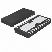
IC FILTER 14MHZ DUAL 22-DFN
Manufacturer
Linear Technology
Datasheet
1.LTC6605CDJC-14PBF.pdf
(20 pages)
Specifications of LTC6605CDJC-14#PBF
Filter Type
Antialiasing
Frequency - Cutoff Or Center
5MHz
Number Of Filters
2
Max-order
2nd
Voltage - Supply
2.7 V ~ 5.25 V
Mounting Type
Surface Mount
Package / Case
22-DFN
No. Of Amplifiers
2
Input Offset Voltage
1mV
Gain Db Max
9.5dB
Bandwidth
14MHz
Supply Voltage Range
2.7V To 5.25V
Supply Current
33.1mA
Amplifier Case Style
DFN
No. Of Pins
22
Rohs Compliant
Yes
Lead Free Status / RoHS Status
Lead free / RoHS Compliant
Available stocks
Company
Part Number
Manufacturer
Quantity
Price


LTC6605-14
PIN FUNCTIONS
+IN2 A, –IN2 A, +IN2 B, –IN2 B (Pins 1, 5, 7, 11): Inputs
to Trimmed 200Ω Resistors. Can accept an input signal,
be fl oated, tied to an output pin, or connected to external
components.
+IN1 A, –IN1 A, +IN1 B, –IN1 B (Pins 2, 4, 8, 10): Inputs
to Trimmed 100Ω Resistors. Can accept an input signal,
be fl oated, tied to an output pin, or connected to external
components.
BIAS A, BIAS B (Pins 3, 9): Three-State Input to Select
Amplifi er Power Consumption. Drive low for shutdown,
drive high for full power, leave fl oating for medium power.
BIAS presents an input resistance of approximately 150k
to a voltage 1.15V above V
V
should be connected to the same voltage, either a ground
plane or a negative supply rail.
8
–
(Pins 6, 14, 17, 20): Negative Supply. All V
–
.
–
pins
V
pins sets the output common mode voltage of each fi lter
channel. If left fl oating, V
midway between V
V
A and B, Respectively. These are not connected to each
other internally.
–OUT A, +OUT A, –OUT B, +OUT B (Pins 22, 18, 16, 12):
Differential Output Pins.
Exposed Pad (Pin 23): Always tie the underlying Exposed
Pad to V
to ground.
OCMA
+
A, V
, V
+
B (Pins 21, 15): Positive Supply for Filter Channel
–
OCMB
. If split supplies are used, do not tie the pad
(Pins 19, 13): The voltage applied to these
+
and V
–
OCM
.
self-biases to a voltage
660514f
Related parts for LTC6605CDJC-14#PBF
Image
Part Number
Description
Manufacturer
Datasheet
Request
R

Part Number:
Description:
IC FILTER 7MHZ DUAL 22-DFN
Manufacturer:
Linear Technology
Datasheet:
Part Number:
Description:
IC FILTER 10MHZ DUAL 22-DFN
Manufacturer:
Linear Technology
Datasheet:
Part Number:
Description:
IC FILTER 10MHZ DUAL 22-DFN
Manufacturer:
Linear Technology
Datasheet:
Part Number:
Description:
IC FILTER 14MHZ DUAL 22-DFN
Manufacturer:
Linear Technology
Datasheet:
Part Number:
Description:
IC FILTER 7MHZ DUAL 22-DFN
Manufacturer:
Linear Technology
Datasheet:

Part Number:
Description:
Dual Matched 10MHz Filter with Low Noise, Low Distortion Differential Amplifi er
Manufacturer:
LINER [Linear Technology]
Datasheet:
Part Number:
Description:
Dual Matched 14MHz Filter with Low Noise, Low Distortion Differential Amplifi er
Manufacturer:
LINER [Linear Technology]
Datasheet:
Part Number:
Description:
Dual Matched 7MHz Filter with Low Noise, Low Distortion Differential Amplifi er
Manufacturer:
LINER [Linear Technology]
Datasheet:

Part Number:
Description:
CD ROM LINEARVIEW DATASHEETS
Manufacturer:
Linear Technology

Part Number:
Description:
Standalone Linear Li-Ion Battery Charger with Thermal Regulation in ThinSOT
Manufacturer:
Linear Technology Corporation
Datasheet:
Part Number:
Description:
Low noise, high frequency, 8th order linear phase lowpass filter
Manufacturer:
Linear Technology Corporation
Datasheet:
Part Number:
Description:
Manufacturer:
Linear Technology Corporation
Datasheet:
Part Number:
Description:
Manufacturer:
Linear Technology Corporation
Datasheet:
Part Number:
Description:
Manufacturer:
Linear Technology Corporation
Datasheet:
Part Number:
Description:
Manufacturer:
Linear Technology Corporation
Datasheet: