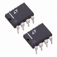
LTC1065CN8 Linear Technology, LTC1065CN8 Datasheet - Page 10

LTC1065CN8
Manufacturer Part Number
LTC1065CN8
Description
IC FILTR 5TH ORDR LOWPASS 8-DIP
Manufacturer
Linear Technology
Datasheet
1.LTC1065CSWPBF.pdf
(16 pages)
Specifications of LTC1065CN8
Filter Type
Bessel, Lowpass Switched Capacitor
Frequency - Cutoff Or Center
50kHz
Number Of Filters
1
Max-order
5th
Voltage - Supply
±2.375 V ~ 8 V
Mounting Type
Through Hole
Package / Case
8-DIP (0.300", 7.62mm)
Lead Free Status / RoHS Status
Contains lead / RoHS non-compliant
The above data is valid for clock frequencies up to 800kHz, 900kHz, 1MHz, for
V
Clock Feedthrough
Clock feedthrough is defined as the RMS value of the clock
frequency and its harmonics which are present at the
filter’s output pin. The clock feedthrough is tested with the
filter input grounded and it depends on the quality of the
PC board layout and power supply decoupling. Any para-
sitic switching transients during the rise and fall of the
incoming clock, are not part of the clock feedthrough
specifications; their amplitude strongly depends on scope
probing techniques as well as ground quality and power
supply bypassing. For a power supply V
feedthrough of the LTC1065 is 50µV
the clock feedthrough approaches 75µV
and 9 show a typical scope photo of the LTC1065 output
pin when the input pin is grounded. The filter cutoff
frequency was 1kHz, while scope bandwidth was chosen
to be 1MHz so that switching transients above the 100kHz
clock frequency would show.
Wideband Noise
The wideband noise data is used to determine the operat-
ing signal-to-noise ratio at a given distortion level. The
wideband noise (µV
of the clock frequency and excludes the clock feedthrough.
The LTC1065’s typical wideband noise is 80µV
9 shows the same scope photo as Figure 8 but with a more
sensitive vertical scale. The clock feedthrough is imbed-
ded in the filter’s wideband noise. The peak-to-peak wide-
band noise of the filter can be clearly seen; it is approxi-
mately 420µV
wideband noise of the part multiplied by a crest factor
of 5.25.
Table 3. CMR Data, f
POWER SUPPLY
A
LTC1065
10
S
= ±2.5V, ±5V, ±7.5V respectively.
PPLICATI
±2.5V
±5V
±7.5V
P-P
±1.8V
∆V
±4V
±6V
. Note that 420µV
O
IN
CLK
RMS
U
= 100kHz
S
– 40°C
84dB
82dB
80dB
) is nearly independent of the value
I FOR ATIO
U
83dB
78dB
77dB
25°C
P-P
RMS
W
equals the 80µV
85°C
80dB
77dB
76dB
S
; for V
= ±5V, the clock
RMS
. Figures 8
RMS
(V
S
OS
= ±7.5V,
U
83dB
78dB
80dB
25°C
. Figure
Nulled)
RMS
Aliasing
Aliasing is an inherent phenomenon of sampled data
filters. It primarily occurs when the frequency of an input
signal approaches the sampling frequency. For the
LTC1065, an input signal whose frequency is in the range
of f
passband and stopband. Table 4 shows details.
Example:
CLK
Figure 9. LTC1065 Output Clock Feedthrough + Noise
Figure 8. LTC1065 Output Clock Feedthrough + Noise
±6% will generate an alias signal into the filter’s
f
CLK
f
CLK
= 100kHz, f
= 100kHz, f
LTC1065, f
f
f
IN
ALIAS
= (19.6kHz, 100mV
C
= (400Hz, 3.16mV
C
= 1kHz, V
= 1kHz, V
CLK
S
S
= ±5V, 1MHz SCOPE BW
2µs/DIV
= ±5V, 1MHz SCOPE BW
2µs/DIV
= 20kHz, f
RMS
RMS
C
)
= 200kHz,
)
1065F08
1063 F09
1065fb


