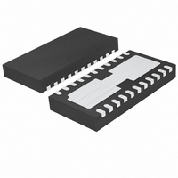
LTC6605CDJC-10#TRPBF Linear Technology, LTC6605CDJC-10#TRPBF Datasheet - Page 14

LTC6605CDJC-10#TRPBF
Manufacturer Part Number
LTC6605CDJC-10#TRPBF
Description
IC FILTER 10MHZ DUAL 22-DFN
Manufacturer
Linear Technology
Datasheet
1.LTC6605CDJC-10PBF.pdf
(20 pages)
Specifications of LTC6605CDJC-10#TRPBF
Filter Type
Antialiasing
Frequency - Cutoff Or Center
5MHz
Number Of Filters
2
Max-order
2nd
Voltage - Supply
2.7 V ~ 5.25 V
Mounting Type
Surface Mount
Package / Case
22-DFN
Lead Free Status / RoHS Status
Lead free / RoHS Compliant
Available stocks
Company
Part Number
Manufacturer
Quantity
Price
Part Number:
LTC6605CDJC-10#TRPBFLTC6605CDJC-10#PBF
Manufacturer:
Linear Technology
Quantity:
135
LTC6605-10
APPLICATIONS INFORMATION
Input Impedance
Calculating the low frequency input impedance depends
on how the inputs are driven.
Figure 6 shows a simplifi ed low frequency equivalent
circuit. For balanced input sources (V
low frequency input impedance is given by the equation:
Therefore, the differential input impedance is simply:
For single-ended inputs (V
increases over the balanced differential case due to the
fact that the summing node (at the junction of R1, R2
and R3) moves in phase with V
impedance. Referring to Figure 6 with V
impedance looking into either input is:
Input Common Mode Voltage Range
The input common mode voltage is defi ned as the average
of the two inputs into resistor R1:
The input common mode range is a function of the fi lter
confi guration (GAIN), V
Referring to Figure 6, the summing junction where R1, R2
and R3 merge together should not swing within 1.4V of
the V
14
R
R
R
V
INP
IN(DIFF)
INCM
INP
+
power supply. Additionally, to avoid forward biasing
V
V
INM
INP
= R
= R
=
+
–
–
+
INM
= 2 • R1
INM
V
R
R
INM
INP
INP
= R1
Figure 6. Input Impedance
+
R1
R1
2
1
V
INM
2
1
INDIFF
R3
R3
•
INM
R1
R1+ R2
R2
R2
+
–
R2
= 0), the input impedance
INP
and the V
to bootstrap the input
INP
INM
660510 F06
0.1μF
OCM
= –V
–
+
= 0, the input
V
V
V
V
OUTDIFF
OUT
OUT
OCM
potential.
INM
–
+
), the
the ESD protection diodes on the input pins, neither input
should swing further than 325mV below the V
rail. Therefore, the input common mode voltage should
be constrained to:
The specifi cations in the Electrical Characteristics table are
a special case of the general equation above. For a single
3V power supply, (V
ΔV
mode range is:
Likewise, for a single 5V power supply, (V
with V
valid input common mode range is:
Output Common Mode and V
The output common mode voltage is defi ned as the aver-
age of the two outputs:
As the equation shows, the output common mode voltage
is independent of the input common mode voltage, and
is instead determined by the voltage on the V
means of an internal feedback loop.
If the V
develops a potential halfway between the V
ages. The V
if desired. For example, when driving an ADC, if the ADC
makes a reference available for setting the common mode
voltage, it can be directly tied to the V
ADC is capable of driving the input impedance presented by
the V
(R
the valid range that can be applied to the V
VOCM
–200mV ≤ V
–200mV ≤ V
V
• V
INDIFF
V
OUTCM
(
OCM
OCM
+
). The Electrical Characteristics table also specifi es
OCM
325mV +
= ±0.25V and R1 = R2, the valid input common
pin as listed in the Electrical Characteristics table
1.4V
= 2.5V, ΔV
OCM
=
pin is left open, an internal resistor divider
V
INCM
INCM
OCM
pin can be overdriven to another voltage
)
V
≤ 1.7V
≤ 4.7V
INDIFF
+
R2
=
R1
2
= 3V, V
INDIFF
V
OUT
V
OCM
+
= ±0.25V and R1 = R2, the
V
OCM
–
+
2
INCM
= 0V) with V
V
OUT
Pin
OCM
−
1+
pin, as long as the
+
= 5V, V
OCM
R2
R1
+
and V
OCM
OCM
pin.
–
= 1.5V,
pin, by
–
power
–
= 0V)
660510f
volt-


