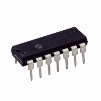
MCP25050-I/P Microchip Technology, MCP25050-I/P Datasheet - Page 42

MCP25050-I/P
Manufacturer Part Number
MCP25050-I/P
Description
IC I/O EXPANDER CAN 8B 14DIP
Manufacturer
Microchip Technology
Specifications of MCP25050-I/P
Mounting Type
Through Hole
Interface
CAN
Number Of I /o
8
Interrupt Output
No
Frequency - Clock
4MHz
Voltage - Supply
2.7 V ~ 5.5 V
Operating Temperature
-40°C ~ 85°C
Package / Case
14-DIP (0.300", 7.62mm)
Includes
ADC, Memory, PWM
Bus Frequency
4MHz
No. Of I/o's
8
Supply Voltage Range
2.7V To 5.5V
Digital Ic Case Style
DIP
No. Of Pins
14
Operating Temperature Range
-40°C To +85°C
Data Rate Max
1Mbps
Leaded Process Compatible
No
Rohs Compliant
Yes
Lead Free Status / RoHS Status
Lead free / RoHS Compliant
For Use With
DV250501 - KIT DEV CAN MCP250XX
Lead Free Status / RoHS Status
Lead free / RoHS Compliant, Lead free / RoHS Compliant
Other names
MCP25050I/P
Available stocks
Company
Part Number
Manufacturer
Quantity
Price
Company:
Part Number:
MCP25050-I/P
Manufacturer:
MIT
Quantity:
6 229
MCP2502X/5X
7.3.2
If the Conversion-on-request mode is selected, the
device performs an A/D conversion only after receiving
a Read A/D Registers or Read Register Receive
message (IRM). In the case of the Read A/D Registers
command, all of the GPIO pins that have been
configured as analog input channels will have an A/D
conversion done before the data frame is sent. When a
Read Register Receive message is initiated (extended
message format only), the A/D conversion is performed
when the MSB of the analog channel is requested, with
the MSB result being transferred. A subsequent read of
the LSB will transmit the value latched when the MSB
was requested (it is recommended that the Read A/D
Registers receive message is used to obtain complete
analog channel values in one message).
REGISTER 7-1:
REGISTER 7-2:
DS21664D-page 42
bit 7-0
bit 7-6
bit 5-0
CONVERSION-ON-REQUEST
MODE
A/D MODULE RESULT REGISTER MSB (ADRES
A/D MODULE RESULT REGISTER LSB (ADRES
AD9:AD2: Most Significant A/D Result bits
Legend:
R = Readable bit
- n = Value at POR
AD1:AD0: Least significant A/D Result bits
Unimplemented: Reads as ‘0’
Legend:
R = Readable bit
- n = Value at POR
bit 7
bit 7
AD9
AD1
R-x
R-x
AD8
AD0
R-x
R-x
AD7
R-x
U-0
—
W = Writable bit
W = Writable bit
‘1’ = Bit is set
‘1’ = Bit is set
AD6
U-0
R-x
—
7.4
Once an A/D auto-conversion has been completed, the
A/D channel result(s) can be compared to a value
stored in the associated A/D channel comparator
registers.
If the value in the analog channel result registers (i.e.,
AN0L and AN10H registers for analog channel 0) is
lower or higher than the value in the A/D comparator
registers (as specified by a corresponding polarity bit),
a transmit-on-change message will be sent (TXID2).
The threshold-detection function for all analog
channels is bit-selectable.
If the A/D channel has been configured for transmit-on-
change mode, the MCP2505 will send a transmit
message with the appropriate data. It is possible that
more than one A/D channel has a change-of-state
condition. This does not pose a problem since all
analog channel data is provided in the transmit
message.
A/D Threshold Detection
U = Unimplemented bit, read as ‘0’
‘0’ = Bit is cleared
U = Unimplemented bit, read as ‘0’
‘0’ = Bit is cleared
AD5
R-x
U-0
—
N
N
L)
H)
AD4
U-0
R-x
© 2007 Microchip Technology Inc.
—
x = Bit is unknown
x = Bit is unknown
AD3
U-0
R-x
—
AD2
U-0
R-x
—
bit 0
bit 0


