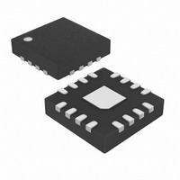
MAX7315ATE+ Maxim Integrated Products, MAX7315ATE+ Datasheet - Page 11

MAX7315ATE+
Manufacturer Part Number
MAX7315ATE+
Description
IC I/O EXPANDER I2C 8B 16TQFN-EP
Manufacturer
Maxim Integrated Products
Datasheet
1.MAX7315ATE.pdf
(26 pages)
Specifications of MAX7315ATE+
Interface
I²C, SMBus
Number Of I /o
8
Interrupt Output
Yes
Frequency - Clock
400kHz
Voltage - Supply
2 V ~ 3.6 V
Operating Temperature
-40°C ~ 125°C
Mounting Type
Surface Mount
Package / Case
16-TQFN Exposed Pad
Operating Supply Voltage
2 V to 3.6 V
Power Dissipation
1176 mW
Operating Temperature Range
- 40 C to + 125 C
Input Voltage
1.08 V to 1.4 V
Maximum Clock Frequency
400 KHz
Mounting Style
SMD/SMT
Output Voltage
0.15 V
Chip Configuration
8 Bit
Bus Frequency
400kHz
Ic Interface Type
I2C, SMBus
No. Of I/o's
8
Supply Voltage Range
2V To 3.6V
Digital Ic Case Style
TQFN
No. Of Pins
16
Filter Terminals
SMD
Rohs Compliant
Yes
Lead Free Status / RoHS Status
Lead free / RoHS Compliant
Any bytes received after the command byte are data
bytes. The first data byte goes into the internal register
of the MAX7315 selected by the command byte (Figure
8). If multiple data bytes are transmitted before a STOP
condition is detected, these bytes are generally stored
in subsequent MAX7315 internal registers because the
command byte address autoincrements (Table 2). A
diagram of a write to the output ports registers (blink
phase 0 register or blink phase 1 register) is given in
Figure 10.
The MAX7315 is read using the MAX7315’s internally
stored command byte as an address pointer the same
way the stored command byte is used as an address
pointer for a write. The pointer autoincrements after
each data byte is read using the same rules as for a
write (Table 2). Thus, a read is initiated by first configur-
ing the MAX7315’s command byte by performing a
write (Figure 7). The master can now read n consecu-
Figure 7. Command Byte Received
Figure 8. Command and Single Data Byte Received
Figure 9. n Data Bytes Received
Control, Interrupt, and Hot-Insertion Protection
S
S
HOW COMMAND BYTE AND DATA BYTE MAP INTO
HOW COMMAND BYTE AND DATA BYTE MAP INTO
S
______________________________________________________________________________________
ACKNOWLEDGE FROM MAX7315
ACKNOWLEDGE FROM MAX7315
SLAVE ADDRESS
SLAVE ADDRESS
8-Port I/O Expander with LED Intensity
MAX7315'S REGISTERS
MAX7315'S REGISTERS
Message Format for Reading
COMMAND BYTE IS STORED ON RECEIPT OF
SLAVE ADDRESS
R/W
R/W
ACKNOWLEDGE FROM MAX7315
0
0
A
A
D15 D14 D13 D12 D11 D10
D15 D14 D13 D12 D11 D10
STOP CONDITION
R/W
0
ACKNOWLEDGE FROM MAX7315
ACKNOWLEDGE FROM MAX7315
COMMAND BYTE
COMMAND BYTE
A
D15
tive bytes from the MAX7315 with the first data byte
being read from the register addressed by the initial-
ized command byte. When performing read-after-write
verification, remember to reset the command byte’s
address because the stored command byte address
has been autoincremented after the write (Table 2). A
diagram of a read from the input ports register is shown
in Figure 10 reflecting the states of the ports.
If the MAX7315 is operated on a 2-wire interface with
multiple masters, a master reading the MAX7315 should
use a repeated start between the write, which sets the
MAX7315’s address pointer, and the read(s) that takes
the data from the location(s) (Table 2). This is because it
is possible for master 2 to take over the bus after master
1 has set up the MAX7315’s address pointer but before
master 1 has read the data. If master 2 subsequently
changes the MAX7315’s address pointer, then master
1’s delayed read can be from an unexpected location.
D14
D9
D9
D8
D8
D13
COMMAND BYTE
A
A
D12
ACKNOWLEDGE FROM MAX7315
Operation with Multiple Masters
D7
D7
D11
AUTOINCREMENT MEMORY ADDRESS
AUTOINCREMENT MEMORY ADDRESS
D6
D6
D10
D5
D5
ACKNOWLEDGE FROM MAX7315
ACKNOWLEDGE FROM MAX7315
DATA BYTE
DATA BYTE
D4
D4
D9
BYTES
BYTE
N
1
D3
D3
D8
D2
D2
A
D1
D1
P
D0
D0
A
A
P
P
11


