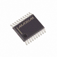
DS4550E+T&R Maxim Integrated Products, DS4550E+T&R Datasheet - Page 15

DS4550E+T&R
Manufacturer Part Number
DS4550E+T&R
Description
IC I/O EXPANDER I2C 9B 20TSSOP
Manufacturer
Maxim Integrated Products
Datasheet
1.DS4550ETR.pdf
(18 pages)
Specifications of DS4550E+T&R
Interface
I²C
Number Of I /o
9
Interrupt Output
No
Frequency - Clock
400kHz
Voltage - Supply
2.7 V ~ 5.5 V
Operating Temperature
-40°C ~ 85°C
Mounting Type
Surface Mount
Package / Case
20-TSSOP
Includes
EEPROM, JTAG
Lead Free Status / RoHS Status
Lead free / RoHS Compliant
Bit Read: At the end a write operation, the master must
release the SDA bus line for the proper amount of setup
time (see
during a bit read. The device shifts out each bit of data
on SDA at the falling edge of the previous SCL pulse
and the data bit is valid at the rising edge of the current
SCL pulse. Remember that the master generates all
SCL clock pulses including when it is reading bits from
the slave.
Acknowledgement
Acknowledgement (ACK) or Not Acknowledge (NACK)
is always the 9th bit transmitted during a byte transfer.
The device receiving data (the master during a read or
the slave during a write operation) performs an ACK by
transmitting a zero during the 9th bit. A device per-
forms a NACK by transmitting a one during the 9th bit.
Timing
all other bit writes. An ACK is the acknowledgment that
the device is properly receiving data. A NACK is used
to terminate a read sequence or as an indication that
the device is not receiving data.
Figure
NOTE: TIMING IS REFERENCED TO V
SDA
SCL
5. I
STOP
(Figure
2
C Timing Diagram
Figure
t
BUF
5) for the ACK and NACK is identical to
START
5) before the next rising edge of SCL
IL(MAX)
t
HD:STA
(ACK
t
LOW
AND V
IH(MIN)
I
and
2
C and JTAG Nonvolatile 9-Bit I/O
____________________________________________________________________
t
R
t
HD:DAT
NACK):
t
F
t
HIGH
An
t
SU:DAT
Expander Plus Memory
Byte Write: A byte write consists of 8 bits of informa-
tion transferred from the master to the slave (most sig-
nificant bit first) plus a 1-bit acknowledgement from the
slave to the master. The 8-bits transmitted by the mas-
ter are done according to the bit write definition and the
acknowledgement is read using the bit read definition.
Byte Read: A byte read is an 8-bit information transfer
from the slave to the master plus a 1-bit ACK or NACK
from the master to the slave. The 8 bits of information
that are transferred (most significant bit first) from the
slave to the master are read by the master using the bit
read definition above, and the master transmits an ACK
using the bit write definition to receive additional data
bytes. The master must NACK the last byte read to ter-
minated communication so the slave returns control of
the SDA to the master.
Slave Address Byte: Each slave on the I
responds to a slave address byte sent immediately fol-
lowing a start condition. The slave address byte con-
tains the slave address in the most significant 7 bits
and the
REPEATED
START
R/W bit in the least significant bit.
t
SU:STA
t
HD:STA
t
SP
t
SU:STO
2
C bus
15


