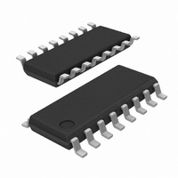
SI2493-C-FS Silicon Laboratories Inc, SI2493-C-FS Datasheet - Page 9

SI2493-C-FS
Manufacturer Part Number
SI2493-C-FS
Description
IC ISOMODEM SYSTEM-SIDE 16SOIC
Manufacturer
Silicon Laboratories Inc
Specifications of SI2493-C-FS
Mfg Application Notes
SI2493/57/34/15/04, Appl Note AN93
Data Format
V.21, V.22, V.23, V.29, V.32, V.34, V.90, V.92, Bell 103, Bell 212A
Baud Rates
56k
Interface
UART
Voltage - Supply
3 V ~ 3.6 V
Mounting Type
Surface Mount
Package / Case
16-SOIC (3.9mm Width)
Lead Free Status / RoHS Status
Lead free / RoHS Compliant
Available stocks
Company
Part Number
Manufacturer
Quantity
Price
Company:
Part Number:
SI2493-C-FSR
Manufacturer:
DY
Quantity:
8 623
Part Number:
SI2493-C-FSR
Manufacturer:
SIEMENS/西门子
Quantity:
20 000
- Current page: 9 of 230
- Download datasheet (7Mb)
2.2. Modem and DAA Operation
This section describes hardware design requirements
for
implementation.
considerations for any hardware design. First, the
reference design and components listed in the
associated bill of materials should be followed exactly.
These designs reflect field experience with millions of
deployed units throughout the world and are optimized
for cost and performance. Any deviation from the
reference design schematic and components will likely
have an adverse affect on performance. Second, circuit
board layouts must rigorously follow " Appendix A—
ISOmodem® Layout Guidelines (Si3018/10)" on page
151. Deviations from these layout techniques will likely
impact modem performance and regulatory compliance.
Finally, all reference designs use a standard component
numbering scheme. This simplifies documentation
references
Laboratories technical support team. It is strongly
recommended that these same component reference
designators be used in all ISOmodem designs.
The following sections describe the operation and
design considerations of the modem chip, DAA chip,
and associated circuitry.
2.2.1. Modem (System-Side) Device
The Si2493/57/34/15/04 modem device contains a
controller, a DSP, program memory (ROM), data
memory (RAM), a serial and parallel interface, a crystal
oscillator, and an isolation capacitor interface.
Note: Parallel, PCM, and EEProm interfaces are only avail-
Figure 2 on page 10 clearly shows that in spite of the
significant internal complexity of the chip, the external
support circuitry is very simple. The following section
describes the function and use of the pins and some
important
placement of components.
optimum
able on the 24-pin TSSOP package option.
considerations
and
Si2493/57/34/15/04
communication
There
for
are
the
with
three
modem
selection
the
important
chipset
Silicon
and
Rev. 0.9
2.2.2. Crystal Oscillator
The crystal oscillator circuit requires a 4.9152 MHz
fundamental mode parallel-resonant crystal. Typical
crystals require a 20 pF load capacitance. This load is
calculated as the series combination of the capacitance
from each crystal terminal to ground including parasitic
capacitance due to package pins and PCB traces. The
parasitic capacitance is estimated as 7 pF per terminal.
This, in combination with the 33 pF capacitor, provides
40 pF per terminal, which, in series, yields the proper
20 pF load for the crystal.
Frequency stability and accuracy are critically important
to the performance of the modem. ITU-T specifications
require less than 200 ppm difference in the carrier
frequency of two modems. This value, split between the
two modems, requires the oscillator frequency of each
modem to be accurate and stable over all operating
conditions within ±100 ppm. This tolerance includes the
initial accuracy of the crystal, frequency drift over the
temperature range the crystal will experience, and five
year aging of the crystal. Other factors affecting the
oscillator
temperature drift of the load capacitor values. For
optimal V.92 performance, it is recommended to
increase the oscillator stability to ±25 ppm.
The CLKIN/XTALI pin (pin 1) can accept a 3.3 V
external 4.9152 MHz clock signal meeting the accuracy
and stability requirements described above. This is the
only input pin on the modem that is not 5 V tolerant. The
Si2493/57/34/04 will accept a 27 MHz clock that meets
the voltage and stability requirements described above.
Enabling this mode of operation is described in Table 24
on page 57.
The CLKOUT/A0 pin (pin 3) outputs a signal derived
from the 4.9152 clock. If the frequency of the output is
controlled via register U6E (CK1) using the Si2404 or
Si2415, this signal is programmable from 2.64 MHz to
40.96 MHz. If using the Si2434 or Si2457, this signal is
programmable from 3.17 MHz to 49.152 MHz. There
are two special cases for the value of R1. If
R1 = 00000b, CLKOUT is disabled. If R1 = 11111b
(default), CLKOUT = 2.048 MHz.
frequency
include
the
tolerance
AN93
and
9
Related parts for SI2493-C-FS
Image
Part Number
Description
Manufacturer
Datasheet
Request
R
Part Number:
Description:
SOIC 16/C�/56 KBPS, V.92 ISOMODEM 16-PIN SYSTEM-SIDE - LEAD-FREE
Manufacturer:
Silicon Laboratories Inc
Part Number:
Description:
TSSOP 24/I�/56 KBPS, V.92 ISOMODEM SYSTEM-SIDE
Manufacturer:
Silicon Laboratories Inc
Part Number:
Description:
IC ISOMODEM SYSTEM-SIDE 24TSSOP
Manufacturer:
Silicon Laboratories Inc
Datasheet:
Part Number:
Description:
56 KBPS, V.92 ISOMODEM SYSTEM-SIDE - LEAD-FREE TSSOP 0 TO 7
Manufacturer:
Silicon Laboratories Inc
Datasheet:
Part Number:
Description:
Telecom ICs CONTACT SILICON LABS FOR AVAILABILITY
Manufacturer:
Silicon Laboratories Inc
Part Number:
Description:
IC ISOMODEM SYSTEM-SIDE 16SOIC
Manufacturer:
Silicon Laboratories Inc
Datasheet:
Part Number:
Description:
IC ISOMODEM SYSTEM-SIDE 24TSSOP
Manufacturer:
Silicon Laboratories Inc
Datasheet:

Part Number:
Description:
IC ISOMODEM W/ERROR CORR 16SOIC
Manufacturer:
Silicon Laboratories Inc
Datasheet:
Part Number:
Description:
IC ISOMODEM W/ERROR CORR 24TSSOP
Manufacturer:
Silicon Laboratories Inc
Datasheet:

Part Number:
Description:
IC ISOMODEM W/DAA 16SOIC
Manufacturer:
Silicon Laboratories Inc
Datasheet:
Part Number:
Description:
IC ISOMODEM SYSTEM-SIDE 24TSSOP
Manufacturer:
Silicon Laboratories Inc
Datasheet:
Part Number:
Description:
IC ISOMODEM W/ERROR CORR 24TSSOP
Manufacturer:
Silicon Laboratories Inc
Datasheet:
Part Number:
Description:
IC ISOMODEM W/DAA 24TSSOP
Manufacturer:
Silicon Laboratories Inc
Datasheet:


