LDS6120NQGI8 IDT, Integrated Device Technology Inc, LDS6120NQGI8 Datasheet - Page 2
LDS6120NQGI8
Manufacturer Part Number
LDS6120NQGI8
Description
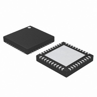
IC SENSOR TCH PURETOUCH 40VFQFPN
Manufacturer
IDT, Integrated Device Technology Inc
Series
PureTouch™r
Type
Capacitive, Keypad LED Driverr
Specifications of LDS6120NQGI8
Number Of Inputs/keys
16 Slider
Data Interface
I²C, Serial, SMBus, SPI™
Voltage - Supply
1.65 V ~ 5.5 V
Operating Temperature
-40°C ~ 85°C
Mounting Type
Surface Mount
Package / Case
40-TQFN
Interface
I²C, SMBus, SPI
Lead Free Status / RoHS Status
Lead free / RoHS Compliant
Current - Supply
-
Output Type
-
Input Type
-
Other names
800-2015-2
Available stocks
Company
Part Number
Manufacturer
Quantity
Price
Company:

Part Number:
LDS6120NQGI8
Manufacturer:
IDT
Quantity:
5 000


IDT
®
LDS6100-6120 PURETOUCH
®
CAPACITANCE TOUCH FAMILY FLYER
Ideal Solution for Portable and “Green” Applications
The LDS6100/6120 is optimized for ultra-low power consumption. In full power mode, sensor conversion
and calibration occur continuously, minimizing the time between touch event and touch detection. With its
ultra-low touch sensor current consumption of <70 μA (typical at 1.8V), the LDS6100 products may be
operated continuously in full power mode, eliminating the need for introduced latencies that can cause
noticeable delays and degrade the user experience. Where power consumption is of the utmost
importance, low power modes with configurable latencies may be utilized to further reduce current
below 25 μA (100ms sleep cycle).
The LDS6100/6120 family is optimized for a minimized solution footprint, with the functionality of multiple
components consolidated into a single device and a bare minimum of required external passive
components. A variety of package options are available including a 4mm x 4mm 28 lead TQFN package, a
5mm x 5mm 40 lead TQFN package (both with 0.75mm package thickness), or a 5.3mm x 10.2mm SSOP
package for applications requiring a wider lead pitch.
*For direct application of 1.8V voltage. For voltages higher than 1.8V, apply voltage to VDDIO and tie VDD1 to ground though C2.
Figure 2. LDS6120 application diagram (typical)
Versatile, accurate CDC
Ultra-low touch sensor power
consumption
Integrated, automatic calibration
algorithms
Integrated touch preference modes
Built-in slider/scroll support
2
• Up to 20 capacitance sensor input channels
• Configurable hysteresis and debounce
• Full power operating mode (typical): <125 μW (VDD1=1.8V)
• Low power operating mode (typical): <50 μW (VDD1=1.8V,
• Shutdown mode (typical): <1 μW (VDD1=1.8V)
• Auto environmental compensation
• Integrated noise immunity algorithms for high-EMI applications
• Strongest single touch / two touches
• Unrestricted (all) touches
• Location, scroll direction, and 2x interpolation supported natively
100ms sleep cycle)
LDS 6100 / 6120 Features
Related parts for LDS6120NQGI8
Image
Part Number
Description
Manufacturer
Datasheet
Request
R

Part Number:
Description:
TRANSLATION DEVICE DPI 80-PQFP
Manufacturer:
IDT, Integrated Device Technology Inc
Datasheet:
Part Number:
Description:
IDT PART
Manufacturer:
IDT, Integrated Device Technology Inc
Datasheet:
Part Number:
Description:
IC LIU T1/E1/J1 OCTAL 256PBGA
Manufacturer:
IDT, Integrated Device Technology Inc
Datasheet:

Part Number:
Description:
IC FREQ TIMING GENERATOR 28TSSOP
Manufacturer:
IDT, Integrated Device Technology Inc
Datasheet:
Part Number:
Description:
IC CLK DVR PLL 1:10 40VFQFPN
Manufacturer:
IDT, Integrated Device Technology Inc
Datasheet:
Part Number:
Description:
IC CLK FANOUT BUFFER 1:18 32LQFP
Manufacturer:
IDT, Integrated Device Technology Inc
Datasheet:
Part Number:
Description:
IC CLK FANOUT BUFFER 1:18 32LQFP
Manufacturer:
IDT, Integrated Device Technology Inc
Datasheet:
Part Number:
Description:
IC CK505 VREG/RES 56TSSOP
Manufacturer:
IDT, Integrated Device Technology Inc
Datasheet:

Part Number:
Description:
IC SDRAM CLK DVR 1:10 48-TSSOP
Manufacturer:
IDT, Integrated Device Technology Inc
Datasheet:

Part Number:
Description:
IC CLK DVR PLL 1:10 48TSSOP
Manufacturer:
IDT, Integrated Device Technology Inc
Datasheet:
Part Number:
Description:
IC FLEXPC CLK PROGR P4 56-TSSOP
Manufacturer:
IDT, Integrated Device Technology Inc
Datasheet:
Part Number:
Description:
IC FLEXPC CLK PROGR P4 56-TSSOP
Manufacturer:
IDT, Integrated Device Technology Inc
Datasheet:
Part Number:
Description:
IC FLEXPC CLK PROGR P4 56-SSOP
Manufacturer:
IDT, Integrated Device Technology Inc
Datasheet:

Part Number:
Description:
IC PLL CLK DRIVER 2.5V 28-TSSOP
Manufacturer:
IDT, Integrated Device Technology Inc
Datasheet:
Part Number:
Description:
IC CLOCK DRIVER 2.5V 24-TSSOP
Manufacturer:
IDT, Integrated Device Technology Inc
Datasheet: