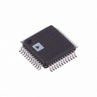
AD9847AKSTZRL Analog Devices Inc, AD9847AKSTZRL Datasheet - Page 17

AD9847AKSTZRL
Manufacturer Part Number
AD9847AKSTZRL
Description
IC CCD SIGNAL PROC 10BIT 48-LQFP
Manufacturer
Analog Devices Inc
Type
CCD Signal Processor, 10-Bitr
Datasheet
1.AD9847AKSTZRL.pdf
(28 pages)
Specifications of AD9847AKSTZRL
Input Type
Logic
Output Type
Logic
Interface
3-Wire Serial
Mounting Type
Surface Mount
Package / Case
48-LQFP
Analog Front End Type
CCD
Analog Front End Category
Video
Interface Type
Serial (3-Wire)
Sample Rate
40MSPS
Input Voltage Range
0.5V
Operating Supply Voltage (min)
2.7/3V
Operating Supply Voltage (typ)
3.3/5V
Operating Supply Voltage (max)
3.6/5.5V
Resolution
10b
Number Of Adc's
1
Power Supply Type
Analog/Digital
Operating Temp Range
-20C to 85C
Operating Temperature Classification
Commercial
Mounting
Surface Mount
Pin Count
48
Package Type
LQFP
Number Of Channels
1
Lead Free Status / RoHS Status
Lead free / RoHS Compliant
Current - Supply
-
Lead Free Status / RoHS Status
Compliant, Lead free / RoHS Compliant
Available stocks
Company
Part Number
Manufacturer
Quantity
Price
Company:
Part Number:
AD9847AKSTZRL
Manufacturer:
Analog Devices Inc
Quantity:
10 000
REV. A
H-Driver and RG Outputs
In addition to the programmable timing positions, the AD9847
features on-chip output drivers for the RG and H1–H4 outputs.
These drivers are powerful enough to directly drive the CCD
inputs. The H-driver current can be adjusted for optimum rise/fall
time into a particular load by using the DRV registers. The RG
drive current is adjustable using the RGDRV register. Each 3-bit
DRV register is adjustable in 3.5 mA increments, with the mini-
mum setting of 0 equal to OFF or three-state and the maximum
setting of 7 equal to 24.5 mA.
As shown in Figure 7, the H2/H4 outputs are inverses of H1/H3.
The internal propagation delay resulting from the signal inversion
is less than 1 ns, which is significantly less than the typical rise
time driving the CCD load. This results in a H1/H2 crossover
voltage at approximately 50% of the output swing. The crossover
voltage is not programmable.
CCD SIGNAL
1 PIXEL PERIOD
POSITION
PERIOD
NOTES
1. ALL SIGNAL EDGES ARE FULLY PROGRAMMABLE TO ANY OF THE 48 POSITIONS WITHIN ONE PIXEL PERIOD.
2. DEFAULT POSITIONS FOR EACH SIGNAL ARE SHOWN ABOVE.
PIXEL
H1/H3
RG
DOUT
CLI
NOTES
1. DIGITAL OUTPUT DATA (DOUT) PHASE IS ADJUSTABLE WITH RESPECT TO THE PIXEL PERIOD.
2. WITHIN 1 CLOCK PERIOD, THE DATA TRANSITION CAN BE PROGRAMMED TO ANY OF THE 48 LOCATIONS.
Figure 6. High Speed Clock Default and Programmable Locations
RGr[0]
Hr[0]
P[0]
P[0]
t
OD
Figure 8. Digital Output Phase Adjustment
RGf[12]
P[12]
P[12]
–17–
P[24]
Hf[24]
Digital Data Outputs
The AD9847 data output phase is programmable using the
DOUTPHASE register. Any edge from 0 to 47 may be programmed,
as shown in Figure 8.
H1/H3
H2/H4
P[24]
SHP[28]
Figure 7. H-Clock Inverse Phase Relationship
t
RISE
P[36]
FIXED CROSSOVER VOLTAGE
P[36]
t
S1
t
PD
<<
t
RISE
P[48] = P[0]
SHD[48]
P[48] = P[0]
H1/H3
AD9847
t
PD
H2/H4


