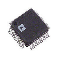
AD9821KST Analog Devices Inc, AD9821KST Datasheet - Page 3

AD9821KST
Manufacturer Part Number
AD9821KST
Description
IC IMAGE SGNL PROC 12BIT 48-LQFP
Manufacturer
Analog Devices Inc
Type
Image Sensorr
Datasheet
1.AD9821KST.pdf
(16 pages)
Specifications of AD9821KST
Rohs Status
RoHS non-compliant
Input Type
Logic
Output Type
Logic
Interface
3-Wire Serial
Mounting Type
Surface Mount
Package / Case
48-LQFP
Analog Front End Type
CCD
Analog Front End Category
Video
Interface Type
Serial (3-Wire)
Sample Rate
40MSPS
Input Voltage Range
0.5V
Operating Supply Voltage (min)
2.7V
Operating Supply Voltage (typ)
3.3V
Operating Supply Voltage (max)
3.6V
Resolution
12b
Number Of Adc's
1
Power Supply Type
Analog/Digital
Operating Temp Range
-20C to 85C
Operating Temperature Classification
Commercial
Mounting
Surface Mount
Pin Count
48
Package Type
LQFP
Number Of Channels
1
Current - Supply
-
Lead Free Status / RoHS Status
Not Compliant
Available stocks
Company
Part Number
Manufacturer
Quantity
Price
Company:
Part Number:
AD9821KST
Manufacturer:
ADI
Quantity:
211
IMAGER-MODE SPECIFICATIONS
Parameter
P
MAXIMUM CLOCK RATE
ANALOG INPUTS (VIN+, VIN–)
VARIABLE GAIN AMPLIFIER (VGA)
BLACK LEVEL CLAMP
SYSTEM PERFORMANCE
POWER-UP RECOVERY TIME
*Input Signal Characteristics defined as follows:
Specifications subject to change without notice.
REV. 0
+1.8V
VIN+
VIN–
GND
OWER CONSUMPTION
Input Common-Mode Range*
Max Input Amplitude*
Max Optical Black Pixel Amplitude*
Gain Control Resolution
Gain Monotonicity
Gain Range
Clamp Level Resolution
Clamp Level
Gain Accuracy
Peak Nonlinearity, 500 mV Input
Total Output Noise
Power Supply Rejection (PSR)
Reference Standby Mode
Total Power-Down Mode
Power-Off Condition
Min Gain (VGA Gain Code 00)
Max Gain (VGA Gain Code 1023)
Min Clamp Level
Max Clamp Level
Min Gain
Max Gain
INPUT SIGNAL RANGE
1V p-p MAX
OB PIXEL
30mV MAX
INPUT
CM RANGE
Min
40
0
1.0
–1
34.5
(T
MIN
to T
Typ
150
± 30
1024
Guaranteed
0
36
256
0
255
0
35.5
0.3
0.5
40
1
3
10
MAX
, AVDD = DVDD = 3.0 V, f
Max
1.8
+1
36.5
–3–
Unit
mW
MHz
V
V p-p
mV
Steps
dB
dB
Steps
LSB
LSB
dB
dB
%
LSB rms
dB
ms
ms
ms
DATACLK
Linear operating range for VIN+, VIN–
Defined as VIN+ minus VIN–
12 dB Gain Applied
AC Grounded Input, 6 dB Gain Applied
Measured with Step Change on Supply
Notes
See TPC 1 for Power vs. Sample Rate
For stable Clamp at max VGA gain
See Figure 11 for VGA Gain Curve
Measured at ADC Output
Specifications Include Entire Signal Chain
Normal Clock Signals Applied
= 40 MHz, unless otherwise noted.)
AD9821


