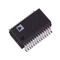
AD9822JRS Analog Devices Inc, AD9822JRS Datasheet - Page 4

AD9822JRS
Manufacturer Part Number
AD9822JRS
Description
IC CCD SIGNAL PROC 14BIT 28-SSOP
Manufacturer
Analog Devices Inc
Type
CCD Signal Processor, 14-Bitr
Datasheet
1.AD9822JRSZRL.pdf
(20 pages)
Specifications of AD9822JRS
Rohs Status
RoHS non-compliant
Input Type
Logic
Output Type
Logic
Interface
3-Wire Serial
Current - Supply
73mA
Mounting Type
Surface Mount
Package / Case
28-SSOP
Analog Front End Type
CCD/CIS
Analog Front End Category
Video
Interface Type
Serial (3-Wire)
Sample Rate
15MSPS
Input Voltage Range
1V
Operating Supply Voltage (min)
3/4.75V
Operating Supply Voltage (typ)
5V
Operating Supply Voltage (max)
5.25V
Resolution
14b
Supply Current
4/73mA
Number Of Adc's
1
Power Supply Type
Analog/Digital
Operating Temp Range
0C to 70C
Operating Temperature Classification
Commercial
Mounting
Surface Mount
Pin Count
28
Package Type
SSOP
Number Of Channels
3
Lead Free Status / RoHS Status
Not Compliant
Available stocks
Company
Part Number
Manufacturer
Quantity
Price
Company:
Part Number:
AD9822JRS
Manufacturer:
AD
Quantity:
1 551
Part Number:
AD9822JRS
Manufacturer:
ADI/亚德诺
Quantity:
20 000
Company:
Part Number:
AD9822JRSRL
Manufacturer:
RENESAS
Quantity:
442
Part Number:
AD9822JRSRL
Manufacturer:
ADI/亚德诺
Quantity:
20 000
Company:
Part Number:
AD9822JRSZ
Manufacturer:
ADI
Quantity:
72
Part Number:
AD9822JRSZ
Manufacturer:
ADI/亚德诺
Quantity:
20 000
Part Number:
AD9822JRSZRL
Manufacturer:
ADI/亚德诺
Quantity:
20 000
AD9822
Parameter
POWER DISSIPATION
1
2
DIGITAL SPECIFICATIONS
T
Table 2.
Parameter
LOGIC INPUTS
LOGIC OUTPUTS
RESET TRANSIENT
Linear input signal range is from 2 V to 4 V when the CCD’s reference level is clamped to 4 V by the AD9822’s input clamp.
The PGA gain is approximately linear-in-dB and follows the equation:
MIN
3-Channel Mode
1-Channel Mode
High Level Input Voltage
Low Level Input Voltage
High Level Input Current
Low Level Input Current
Input Capacitance
High Level Output Voltage
Low Level Output Voltage
High Level Output Current
Low Level Output Current
3-Channel Mode @ 6 MHz
1-Channel Mode @ 6 MHz
1V TYP
to T
MAX
, AVDD = 5 V, DRVDD = 5 V, CDS mode, f
2V p-p MAX INPUT SIGNAL RANGE
4V SET BY INPUT CLAMP (3V OPTION ALSO AVAILABLE)
ADCCLK
Gain
Rev. B | Page 4 of 20
= 15 MHz, f
Symbol
V
V
I
I
C
V
V
I
I
=
IH
IL
OH
OL
IH
IL
IN
OH
OL
[
Min
1
+
4
7 .
5
⎡
⎢
⎣
7 .
63
CDSCLK1
63
−
G
⎤
⎥
⎦
]
= f
where G is the register value. See Figure
CDSCLK2
Typ
385
335
300
250
Min
2.0
4.5
= 5 MHz, C
Typ
10
10
10
50
50
L
= 10 pF, unless otherwise noted.
Max
450
410
Max
0.8
0.1
15
.
Unit
mW
mW
mW
mW
Unit
V
V
µA
µA
pF
V
V
µA
µA


