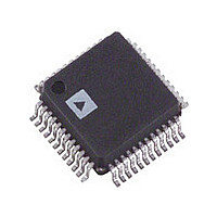
AD9845AJST Analog Devices Inc, AD9845AJST Datasheet - Page 5

AD9845AJST
Manufacturer Part Number
AD9845AJST
Description
IC CCD SIGNAL PROC 12BIT 48-LQFP
Manufacturer
Analog Devices Inc
Type
CCD Signal Processor, 12-Bitr
Datasheet
1.AD9845AJST.pdf
(22 pages)
Specifications of AD9845AJST
Rohs Status
RoHS non-compliant
Input Type
Logic
Output Type
Logic
Interface
3-Wire Serial
Mounting Type
Surface Mount
Package / Case
48-LQFP
Current - Supply
-
Lead Free Status / RoHS Status
Not Compliant
Available stocks
Company
Part Number
Manufacturer
Quantity
Price
Part Number:
AD9845AJST
Manufacturer:
AD
Quantity:
20 000
TIMING SPECIFICATIONS
Parameter
SAMPLE CLOCKS
DATA OUTPUTS
SERIAL INTERFACE
NOTES
1
Specifications subject to change without notice.
ABSOLUTE MAXIMUM RATINGS
Parameter
AVDD1, AVDD2
DVDD1, DVDD2
DRVDD
Digital Outputs
SHP, SHD, DATACLK
CLPOB, CLPDM, PBLK DVSS
SCK, SL, SDATA
VRT, VRB, CMLEVEL
BYP1-4, CCDIN
Junction Temperature
Lead Temperature
CAUTION
ESD (electrostatic discharge) sensitive device. Electrostatic charges as high as 4000 V readily
accumulate on the human body and test equipment and can discharge without detection. Although
the AD9845A features proprietary ESD protection circuitry, permanent damage may occur on
devices subjected to high-energy electrostatic discharges. Therefore, proper ESD precautions are
recommended to avoid performance degradation or loss of functionality.
Minimum CLPOB pulsewidth is for functional operation only. Wider typical pulses are recommended to achieve low noise clamp performance.
DATACLK, SHP, SHD Clock Period
DATACLK Hi/Low Pulsewidth
SHP Pulsewidth
SHD Pulsewidth
CLPDM Pulsewidth
CLPOB Pulsewidth
SHP Rising Edge to SHD Falling Edge
SHP Rising Edge to SHD Rising Edge
Internal Clock Delay
Inhibited Clock Period
Output Delay
Output Hold Time
Pipeline Delay
Maximum SCK Frequency
SL to SCK Setup Time
SCK to SL Hold Time
SDATA Valid to SCK Rising Edge Setup
SCK Falling Edge to SDATA Valid Hold
SCK Falling Edge to SDATA Valid Read
(10 sec)
1
With
Respect
To
AVSS
DVSS
DRVSS
DRVSS
DVSS
DVSS
AVSS
AVSS
Min Max
–0.3 +3.9
–0.3 +3.9
–0.3 +3.9
–0.3 DRVDD + 0.3 V
–0.3 DVDD + 0.3
–0.3 DVDD + 0.3
–0.3 DVDD + 0.3
–0.3 AVDD + 0.3
–0.3 AVDD + 0.3
(C
Serial Timing in Figures 26–29.)
L
= 20 pF, f
150
300
SAMP
= 30 MHz, CCD-Mode Timing in Figures 10 and 11, AUX-Mode Timing in Figure 7.
Unit
V
V
V
V
V
V
V
V
°C
°C
Symbol
t
t
t
t
t
t
t
t
t
t
t
t
f
t
t
t
t
t
SCLK
CONV
ADC
SHP
SHD
CDM
COB
S1
S2
ID
INH
OD
H
LS
LH
DS
DH
DV
Model
AD9845AJST –20°C to +85°C
THERMAL CHARACTERISTICS
Thermal Resistance
48-Lead LQFP Package
θ
JA
= 92°C
Min
32
13
5
5
4
2
0
13
10
7.0
10
10
10
10
10
10
Temperature
Range
ORDERING GUIDE
Typ
33
16.7
8.3
8.3
10
20
8.3
16.7
3.0
14.5
7.6
9
WARNING!
Max
16
Package
Description
Thin Plastic
Quad Flatpack
(LQFP)
ESD SENSITIVE DEVICE
AD9845A
Package
Option
ST-48
Unit
ns
ns
ns
ns
Pixels
Pixels
ns
ns
ns
ns
ns
ns
Cycles
MHz
ns
ns
ns
ns
ns


