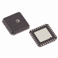
AD9945KCP Analog Devices Inc, AD9945KCP Datasheet - Page 8

AD9945KCP
Manufacturer Part Number
AD9945KCP
Description
IC CCD SIGNAL PROCESSOR 32-LFCSP
Manufacturer
Analog Devices Inc
Type
CCD Signal Processor, 12-Bitr
Specifications of AD9945KCP
Rohs Status
RoHS non-compliant
Input Type
Logic
Output Type
Logic
Interface
3-Wire Serial
Mounting Type
Surface Mount
Package / Case
32-LFCSP
Analog Front End Type
CCD
Analog Front End Category
Video
Interface Type
Serial (3-Wire)
Sample Rate
40MSPS
Input Voltage Range
0.5V
Operating Supply Voltage (min)
2.7V
Operating Supply Voltage (typ)
3V
Operating Supply Voltage (max)
3.6V
Resolution
12b
Number Of Adc's
1
Power Supply Type
Analog/Digital
Operating Temp Range
-20C to 85C
Operating Temperature Classification
Commercial
Mounting
Surface Mount
Pin Count
32
Package Type
LFCSP EP
Number Of Channels
1
Current - Supply
-
Lead Free Status / RoHS Status
Not Compliant
Available stocks
Company
Part Number
Manufacturer
Quantity
Price
Company:
Part Number:
AD9945KCP
Manufacturer:
ADI
Quantity:
455
Company:
Part Number:
AD9945KCPZ
Manufacturer:
ADI44
Quantity:
300
Part Number:
AD9945KCPZ
Manufacturer:
ADI/亚德诺
Quantity:
20 000
Part Number:
AD9945KCPZRL7
Manufacturer:
ADI/亚德诺
Quantity:
20 000
AD9945
INTERNAL REGISTER DESCRIPTION
Register
Name
Operation
Control
Clamp Level
VGA Gain
Startup
NOTE: All register values default to 0x0000 at power-up except clamp level, which defaults to 128 decimal (128 LSB clamp level).
A3 A2 A1 A0
0
0
Address Bits
0
1
0
0
0
0
1
0
0
0
1
1
0
0
1
1
1
0
Data Bits
D0
D2, D1
D3
D5, D4
D6
D8, D7
D11 to D9
D0
D1
D2
D3
D4
D5
D6
D11 to D7
D7 to D0
D9 to D0
D11 to D0
Function
Software Reset (0 = Normal Operation, 1 = Reset all registers to default)
Power-Down Modes (00 = Normal Power, 01 = Standby, 10 = Total Shutdown)
OB Clamp Disable (0 = Clamp ON, 1 = Clamp OFF)
Test Mode. Should always be set to 00.
PBLK Blanking Level (0 = Blank Output to Zero, 1 = Blank to OB Clamp Level)
SHP/SHD Input Polarity (0 = Active Low, 1 = Active High)
DATACLK Input Polarity (0 = Active Low, 1 = Active High)
CLPOB Input Polarity (0 = Active Low, 1 = Active High)
PBLK Input Polarity (0 = Active Low, 1 = Active High)
Three-State Data Outputs (0 = Outputs Active, 1 = Outputs Three-Stated)
Data Output Latching (0 = Latched by DATACLK, 1 = Latch is Transparent)
Data Output Coding (0 = Binary Output, 1 = Gray Code Output)
Test Mode. Should always be set to 00000.
OB Clamp Level (0 = 0 LSB, 255 = 255 LSB)
VGA Gain (0 = 6 dB, 1023 = 40 dB)
Required start-up write must be set to 0x838.
Table I. Internal Register Map
Test Mode. Should always be set to 000.
Low Gain Mode. Normally set to 00. To enable low gain mode, set to 11. When low gain mode
is enabled, VGA Gain register must be set to all zeroes.
–8–
REV. B


