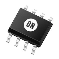
NCV1124DG ON Semiconductor, NCV1124DG Datasheet - Page 2

NCV1124DG
Manufacturer Part Number
NCV1124DG
Description
IC SENSOR DUAL VAR-RELUCT 8-SOIC
Manufacturer
ON Semiconductor
Type
Variable Reluctancer
Datasheet
1.NCV1124DG.pdf
(8 pages)
Specifications of NCV1124DG
Input Type
Logic
Output Type
Logic
Interface
Dual, Serial or Parallel
Current - Supply
5mA
Mounting Type
Surface Mount
Package / Case
8-SOIC (3.9mm Width)
Mounting Style
SMD/SMT
Ic Function
Dual Variable-Reluctance Sensor Interface IC
Supply Voltage Range
4.5V To 5.5V
Operating Temperature Range
-40°C To +125°C
Digital Ic Case Style
SOIC
No. Of Pins
8
Termination Type
SMD
Rohs Compliant
Yes
Filter Terminals
SMD
Lead Free Status / RoHS Status
Lead free / RoHS Compliant
Other names
NCV1124DG
NCV1124DGOS
NCV1124DGOS
Available stocks
Company
Part Number
Manufacturer
Quantity
Price
Company:
Part Number:
NCV1124DG
Manufacturer:
ON Semiconductor
Quantity:
591
Company:
Part Number:
NCV1124DG
Manufacturer:
Diodes
Quantity:
2 498
Part Number:
NCV1124DG
Manufacturer:
ON/安森美
Quantity:
20 000
Stresses exceeding Maximum Ratings may damage the device. Maximum Ratings are stress ratings only. Functional operation above the
Recommended Operating Conditions is not implied. Extended exposure to stresses above the Recommended Operating Conditions may affect
device reliability.
1. 60 second maximum above 183°C.
2. This parameter is guaranteed by design, but not parametrically tested in production.
MAXIMUM RATINGS
ELECTRICAL CHARACTERISTICS
V
Sensor Inputs
Logic Inputs
Storage Temperature Range
Ambient Operating Temperature
Supply Voltage Range (continuous)
Input Voltage Range (at any input, R1 = R2 = 22 k)
Maximum Junction Temperature
ESD Susceptibility (Human Body Model)
Lead Temperature Soldering:
Operating Current Supply
Input Threshold − Positive
Input Threshold − Negative
Input Bias Current (INP1, INP2)
Input Bias Current (DIAG)
Input Bias Current Factor (K
Bias Current Matching
Input Clamp − Negative
Input Clamp − Positive
Output Low Voltage
Output High Voltage
Mode Change Time Delay
Input to Output Delay
Output Rise Time
Output Fall Time
Open−Sensor Positive Threshold
DIAG Input Low Threshold
DIAG Input High Threshold
DIAG Input Resistance
CC
(IN
SUPPLY
Adj
= INP × K
Characteristic
I
)
I
)
(4.5 V < V
V
V
V
V
V
V
V
V
V
INP1 or INP2 to IN
I
I
I
I
I
I
C
C
V
V
V
IN
IN
IN
OUT
OUT
OUT
CC
DIAG
DIAG
DIAG
DIAG
IN
DIAG
IN
IN
LOAD
LOAD
DIAG
IN
IN
Rating
= −50 mA
= −12 mA
= +12 mA
= 0.336 V
= 0.336 V, V
= 0.336 V, V
= 0.3 × V
= V
= 5.0 V
= 1.6 mA
= −1.6 mA
= 1.0 mA
= Low
= High
= Low
= High
= 0 V
= High, R
= 30 pF
= 30 pF
CC
CC
Test Conditions
, V
< 5.5 V, −40°C < T
http://onsemi.com
CC
CC
IN(Adj)
DIAG
DIAG
= 5.0 V
, V
−
−
−
NCV1124
Adj
CC
Reflow: (SMD styles only) (Note 1)
= Low
= High
, V
= 40 k. Note 2
= 5.0 V
2
IN
= 0.336 V
A
< 125°C, V
V
0.7 × V
CC
DIAG
−185
−1.0
−0.5
−0.5
29.4
Min
135
135
135
−16
152
5.0
8.0
8.0
−
−
−
−
0
−
−
−
−
− 0.5
CC
= 0; unless otherwise specified.)
V
CC
−0.25
−0.30
−160
0.05
Typ
160
160
160
100
155
−11
7.0
0.2
1.0
0.5
54
22
22
−
−
0
−
−
−
− 0.2
−250 to 250
−65 to 150
−40 to 125
−0.3 to 7.0
240 peak
Value
150
2.0
0.2 × V
−135
Max
−6.0
86.9
185
185
185
157
5.0
1.0
1.0
9.8
0.4
2.0
2.0
20
20
70
70
−
0
0
−
−
CC
%INP
%INP
Unit
Unit
mA
mV
mV
mV
mV
mA
mA
mA
kW
kW
kW
°C
°C
°C
kV
°C
ms
ms
ms
ms
V
V
V
V
V
V
V
V
V


