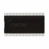
FIN3385MTDX Fairchild Semiconductor, FIN3385MTDX Datasheet - Page 3

FIN3385MTDX
Manufacturer Part Number
FIN3385MTDX
Description
IC SERIALIZER/DESERIAL 56-TSSOP
Manufacturer
Fairchild Semiconductor
Type
Low Voltage 28-Bit Flat Panel Display Linkr
Datasheet
1.FIN3384MTDX.pdf
(21 pages)
Specifications of FIN3385MTDX
Function
Serializer/Deserializer
Data Rate
2.38Gbps
Input Type
LVTTL
Output Type
LVDS
Number Of Inputs
28
Number Of Outputs
4
Voltage - Supply
3 V ~ 3.6 V
Operating Temperature
-10°C ~ 70°C
Mounting Type
Surface Mount
Package / Case
56-TSSOP
Ic Output Type
LVDS
No. Of Inputs
28
No. Of Outputs
4
Supply Voltage Range
3V To 3.6V
Driver Case Style
TSSOP
No. Of Pins
56
Termination Type
SMD
Rohs Compliant
Yes
Number Of Drivers
4
Number Of Receivers
28
Operating Supply Voltage
3.3 V
Maximum Operating Temperature
+ 150 C
Minimum Operating Temperature
- 65 C
Mounting Style
SMD/SMT
Supply Current
41.8 mA
Supply Voltage (max)
3.6 V
Supply Voltage (min)
3 V
Filter Terminals
SMD
Digital Ic Case Style
TSSOP
Lead Free Status / RoHS Status
Lead free / RoHS Compliant
Other names
FIN3385MTDX
FIN3385MTDXTR
FIN3385MTDXTR
© 2003 Fairchild Semiconductor Corporation
FIN3383/3384/3385/3386 • Rev. 1.0.4
Transmitters
Pin Configuration
Pin Definitions
Figure 3. FIN3383 and FIN3385 (28:4 Transmitter)
Pin Names
TxCLKOut+
LVDS GND
TxCLKOut-
LVDS V
PLL GND
TxCLKIn
PLL V
TxOut+
/PwrDn
TxOut-
R_FB
GND
TxIn
V
CC
CC
CC
I/O Types
O
O
O
O
I
I
I
I
I
I
I
I
I
I
Pin Assignment
Number of Pins
28/21
4/3
4/3
1
1
2
1
3
3
5
1
1
1
1
LVTTL Level Input
LVTTL Level Clock Input, the rising edge is for data strobe
Positive LVDS Differential Data Output
Negative LVDS Differential Data Output
Positive LVDS Differential Clock Output
Negative LVDS Differential Clock Output
Rising Edge Data Strobe: Assert HIGH (V
Falling Edge Data Strobe: Assert LOW (Ground)
LVTTL Level Power-Down Input Assertion (LOW) puts the
outputs in high-impedance state
Power Supply Pin for PLL
Ground Pins for PLL
Power Supply Pin for LVDS Output
Ground Pins for LVDS Output
Power Supply Pins for LVTTL Input
Ground Pin for LVTTL Input
3
Truth Table
Notes:
Floating
Floating
1.
2.
Active
Active
Don’t
Care
TxIn
The outputs of the transmitter or receiver
remains in a high-impedance state until V
reaches 2V.
TxCLKOut± settles at a free-running frequency
when the part is powered up, /PwrDn is HIGH,
and the TxCLKIn is a steady logic level (LOW /
HIGH / High-Impedance).
HIGH/ High
Impedance
Don’t Care
Description of Signals
TxCLKIn
Floating
Inputs
Active
Active
LOW/
/PwrDn
HIGH
HIGH
HIGH
HIGH
LOW
(1)
Impedance
TxOut±
CC
LOW/
HIGH
LOW/
HIGH
LOW
LOW
High
)
Outputs
www.fairchildsemi.com
TxCLKOut±
Impedance
Care
Care
LOW/
LOW/
HIGH
HIGH
Don’t
Don’t
High
CC
(2)
(2)


