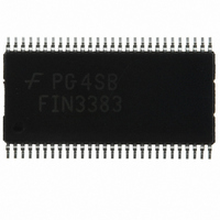
FIN3383MTDX Fairchild Semiconductor, FIN3383MTDX Datasheet - Page 7
FIN3383MTDX
Manufacturer Part Number
FIN3383MTDX
Description
IC SERIALIZER/DESERIAL 56-TSSOP
Manufacturer
Fairchild Semiconductor
Datasheet
1.FIN3384MTDX.pdf
(21 pages)
Specifications of FIN3383MTDX
Function
Serializer/Deserializer
Data Rate
2.38Gbps
Input Type
LVTTL
Output Type
LVDS
Number Of Inputs
28
Number Of Outputs
4
Voltage - Supply
3 V ~ 3.6 V
Operating Temperature
-10°C ~ 70°C
Mounting Type
Surface Mount
Package / Case
56-TSSOP
Lead Free Status / RoHS Status
Lead free / RoHS Compliant
Other names
FIN3383MTDX
FIN3383MTDXTR
FIN3383MTDXTR


© 2003 Fairchild Semiconductor Corporation
FIN3383/3384/3385/3386 • Rev. 1.0.4
Transmitter DC Electrical Characteristics
Typical values are at T
temperatures ranges, unless otherwise specified.
Transmitter LVTTL Input Characteristics
Transmitter LVDS Output Characteristics
Transmitter Supply Current
Notes:
9.
10. The power supply current for both transmitter and receiver can vary with the number of active I/O channels.
11. The 16-grayscale test pattern tests device power consumption for a “typical” LCD display pattern. The test
Symbol
I
ΔV
I
ΔV
I
CCPDT
CCWT
V
V
CCGT
V
V
V
I
Positive current values refer to the current flowing into device and negative values means current flowing out of
pins. Voltages are referenced to ground unless otherwise specified (except ΔV
pattern approximates signal switching needed to produce groups of 16 vertical strips across the display.
I
I
OS
OZ
IN
OD
OS
IH
IK
IL
OD
OS
Input HIGH Voltage
Input LOW Voltage
Input Clamp Voltage
Input Current
Output Differential Voltage
V
LOW-to-HIGH
Offset Voltage
Offset Magnitude Change from
Differential LOW-to-HIGH
Short-Circuit Output Current
Disabled Output Leakage Current
28:4 Transmitter Power Supply Current
for Worst-Case Pattern (with Load)
Powered-Down Supply Current
28:4 Transmitter Supply Current for 16
Grayscale
OD
Magnitude Change from Differential
A
=25°C and with V
(10)
Parameter
CC
=3.3V; minimum and maximum are at over supply voltages and operating
(9)
(10)
7
I
V
V
R
Figure 5
V
DO=0V to 4.6V,
/PwrDn=0V
R
Figure 8
/PwrDn=0.8V
Figure
23
IK
IN
IN
L
OUT
L
=-18mA
=100Ω,
=100Ω
(11)
=0.4V to 4.6V
=GND
Conditions
=0V
32.5MHz
32.5MHz
40MHz
66MHz
85MHz
40MHz
66MHz
85MHz
1.125
Min.
GND
250
2.0
-10
OD
and V
1.250
Typ.
-0.79
31.0
32.0
37.0
42.0
10.0
29.0
30.0
35.0
39.0
OD
-3.5
1.8
25
±1
0
).
Max.
1.375
-1.50
10.0
49.5
55.0
60.5
66.0
55.0
41.8
44.0
49.5
55.0
450
-5.0
±10
V
0.8
35
www.fairchildsemi.com
CC
Units
mV
mV
mV
mA
mA
mA
µA
µA
µA
V
V
V
V
Related parts for FIN3383MTDX
Image
Part Number
Description
Manufacturer
Datasheet
Request
R

Part Number:
Description:
Low Voltage 28-Bit Flat Panel Display Link Serializers
Manufacturer:
FAIRCHILD [Fairchild Semiconductor]
Datasheet:

Part Number:
Description:
(FIN3383 - FIN3386) Low Voltage 28-Bit Flat Panel Display Link Serializers/Deserializers
Manufacturer:
Fairchild Semiconductor
Datasheet:
Part Number:
Description:
Fairchild Semiconductor [IGBT MODULE]
Manufacturer:
Fairchild Semiconductor
Datasheet:

Part Number:
Description:
Discrete Semiconductor Modules
Manufacturer:
Fairchild Semiconductor
Part Number:
Description:
Discrete Semiconductor Modules
Manufacturer:
Fairchild Semiconductor
Part Number:
Description:
This N-Channel MOSFET is produced using Fairchild Semiconductor’s advanced Power Trench® process
Manufacturer:
Fairchild Semiconductor
Datasheet:
Part Number:
Description:
This N-Channel MOSFET is produced using Fairchild Semiconductor’s advanced Power Trench® process
Manufacturer:
Fairchild Semiconductor
Datasheet:
Part Number:
Description:
This N-Channel MOSFET is produced using Fairchild Semiconductor’s advanced PowerTrench® process
Manufacturer:
Fairchild Semiconductor
Datasheet:
Part Number:
Description:
This N-Channel MOSFET is produced using Fairchild Semiconductor’s advanced PowerTrench® process
Manufacturer:
Fairchild Semiconductor
Datasheet:
Part Number:
Description:
This N-Channel MOSFET is produced using Fairchild Semiconductor’s advanced Power Trench® process
Manufacturer:
Fairchild Semiconductor
Datasheet:
Part Number:
Description:
This N-Channel logic Level MOSFETs are produced using Fairchild Semiconductor‘s advanced Power Trench® process that has been special tailored to minimize the on-state resistance and yet maintain superior switching performance
Manufacturer:
Fairchild Semiconductor
Datasheet:
Part Number:
Description:
This N-Channel MOSFET is produced using Fairchild Semiconductor’s advanced Power Trench® process
Manufacturer:
Fairchild Semiconductor
Datasheet:
Part Number:
Description:
This N-Channel SyncFET™ is produced using Fairchild Semiconductor’s advanced PowerTrench® process
Manufacturer:
Fairchild Semiconductor
Datasheet:
Part Number:
Description:
This N-Channel SyncFET™ is produced using Fairchild Semiconductor’s advanced PowerTrench® process
Manufacturer:
Fairchild Semiconductor
Datasheet:
Part Number:
Description:
This N-Channel SyncFET™ is produced using Fairchild Semiconductor’s advanced PowerTrench® process
Manufacturer:
Fairchild Semiconductor
Datasheet: