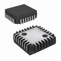
CLC020BCQ/NOPB National Semiconductor, CLC020BCQ/NOPB Datasheet - Page 13

CLC020BCQ/NOPB
Manufacturer Part Number
CLC020BCQ/NOPB
Description
IC SERIALIZER VIDEO DGTL 28-PLCC
Manufacturer
National Semiconductor
Datasheet
1.CLC020BCQNOPB.pdf
(15 pages)
Specifications of CLC020BCQ/NOPB
Function
Serializer
Data Rate
400Mbps
Input Type
CMOS
Output Type
CMOS, TTL
Number Of Inputs
10
Number Of Outputs
1
Voltage - Supply
4.5 V ~ 5.5 V
Operating Temperature
0°C ~ 70°C
Mounting Type
Surface Mount
Package / Case
28-PLCC
For Use With
SD020EVK - BOARD EVALUATION CLC020
Lead Free Status / RoHS Status
Lead free / RoHS Compliant
Other names
*CLC020BCQ
*CLC020BCQ/NOPB
CLC020BCQ
*CLC020BCQ/NOPB
CLC020BCQ
Available stocks
Company
Part Number
Manufacturer
Quantity
Price
Company:
Part Number:
CLC020BCQ/NOPB
Manufacturer:
National Semiconductor
Quantity:
135
Company:
Part Number:
CLC020BCQ/NOPB
Manufacturer:
LT
Quantity:
4 067
Company:
Part Number:
CLC020BCQ/NOPB
Manufacturer:
Texas Instruments
Quantity:
10 000
Application Information
PCB LAYOUT AND POWER SYSTEM BYPASS
RECOMMENDATIONS
Circuit board layout and stack-up for the CLC020 should be
designed to provide noise-free power to the device. Good
layout practice also will separate high frequency or high level
inputs and outputs to minimize unwanted stray noise pickup,
feedback and interference. Power system performance may
be greatly improved by using thin dielectrics (4 to 10 mils) for
power/ground sandwiches. This increases the intrinsic ca-
pacitance of the PCB power system which improves power
supply filtering, especially at high frequencies, and makes
the value and placement of external bypass capacitors less
critical. External bypass capacitors should include both RF
ceramic and tantalum electrolytic types. RF capacitors may
use values in the range 0.01 µF to 0.1 µF. Tantalum capaci-
tors may be in the range 2.2 µF to 10 µF. Voltage rating for
tantalum capacitors should be at least 5x the power supply
voltage being used. It is recommended practice to use two
vias at each power pin of the CLC020 as well as all RF
bypass capacitor terminals. Dual vias reduce the intercon-
nect inductance by up to half, thereby reducing interconnect
inductance and extending the effective frequency range of
the bypass components.
The outer layers of the PCB may be flooded with additional
V
isolation as well as increase the intrinsic capacitance of the
power supply plane system. Naturally, to be effective, these
planes must be tied to the V
quent intervals with vias. Frequent via placement also im-
proves signal integrity on signal transmission lines by pro-
SS
(ground) plane. These planes will improve shielding and
SS
power supply plane at fre-
(Continued)
FIGURE 11. Jitter Plots
13
viding short paths for image currents which reduces signal
distortion. The planes should be pulled back from all trans-
mission lines and component mounting pads a distance
equal to the width of the widest transmission line or the
thickness of the dielectric separating the transmission line
from the internal power or ground plane(s) whichever is
greater. Doing so minimizes effects on transmission line
impedances and reduces unwanted parasitic capacitances
at component mounting pads.
In especially noisy power supply environments, such as is
often the case when using switching power supplies, sepa-
rate filtering may be used at the CLC020’s VCO and output
driver power pins. The CLC020 was designed for this situa-
tion. The digital section, VCO and output driver power supply
feeds are independent (see pinout description table and
pinout drawing for details). Supply filtering may take the form
of L-section or pi-section, L-C filters in series with these V
inputs. Such filters are available in a single package from
several manufacturers. Despite being independent feeds, all
device power supplies should be applied simultaneously as
from a common source. The CLC020 is free from power
supply latch-up caused by circuit-induced delays between
the device’s three separate power feed systems.
REPLACING THE GENNUM GS9022
The CLC020 is form-fit-function compatible with the Gennum
GS9022. The CLC020 can improve the performance of
GS9022 applications using the existing PCB layout with the
removal of certain components or changes to component
10091711
www.national.com
DD


