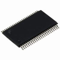
FIN1216MTDX Fairchild Semiconductor, FIN1216MTDX Datasheet - Page 11

FIN1216MTDX
Manufacturer Part Number
FIN1216MTDX
Description
IC SERIALIZER/DESERIAL 48-TSSOP
Manufacturer
Fairchild Semiconductor
Datasheet
1.FIN1215MTDX.pdf
(20 pages)
Specifications of FIN1216MTDX
Function
Serializer/Deserializer
Data Rate
1.785Gbps
Input Type
LVDS
Output Type
LVTTL
Number Of Inputs
3
Number Of Outputs
21
Voltage - Supply
3 V ~ 3.6 V
Operating Temperature
-40°C ~ 85°C
Mounting Type
Surface Mount
Package / Case
48-TSSOP
Lead Free Status / RoHS Status
Lead free / RoHS Compliant
Other names
FIN1216MTDX
FIN1216MTDXTR
FIN1216MTDXTR
Available stocks
Company
Part Number
Manufacturer
Quantity
Price
© 2003 Fairchild Semiconductor Corporation
FIN1215 / FIN1216 / FIN1217 • Rev. 1.0.3
Receiver AC Electrical Characteristics
Values are at over supply voltages and operating temperatures, unless otherwise specified.
Symbol
t
t
t
t
t
t
t
t
t
t
t
t
t
t
t
t
t
t
t
t
t
t
t
t
t
RSPB0
RSPB1
RSPB2
RSPB3
RSPB4
RSPB5
RSPB6
RCOH
RCOH
RCOH
RCOL
RSRC
RHRC
RCOP
RCOL
RSRC
RHRC
RCOP
RCOL
RSRC
RHRC
ROLH
ROHL
RCCD
RPDD
RxCLKOut LOW Time
RxCLKOut HIGH Time
RxOut Valid Prior to RxCLKOut
RxOut Valid After RxCLKOut
Receiver Clock Output (RxCLKOut)
Period
RxCLKOut LOW Time
RxCLKOut HIGH Time
RxOut Valid Prior to RxCLKOut
RxOut Valid After RxCLKOut
Receiver Clock Output (RxCLKOut)
Period
RxCLKOut LOW Time
RxCLKOut HIGH Time
RxOut Valid Prior to RxCLKOut
RxOut Valid After RxCLKOut
Output Rise Time (20% to 80%)
Output Fall Time (80% to 20%)
Receiver Clock Input to Clock Output
Delay
Receiver Power-Down Delay
Receiver Input Strobe Position of Bit 0
Receiver Input Strobe Position of Bit 1
Receiver Input Strobe Position of Bit 2
Receiver Input Strobe Position of Bit 3
Receiver Input Strobe Position of Bit 4
Receiver Input Strobe Position of Bit 5
Receiver Input Strobe Position of Bit 6
Parameter
11
Figure 12
Rising Edge Strobe
f=40MHz
Figure 12
Rising Edge Strobe
f=65MHz
Figure 12
Rising Edge Strobe
f=85MHz
FIN1218 only
C
T
Figure 14
Reference source not found.)
Figure 18
Figure 21
f=40MHz
A
L
=25°C, V
=8pF, Figure 9
Conditions
(Error!
CC
=3.3V
11.76
Min.
10.0
10.0
15.0
1.00
8.10
11.6
15.1
18.8
22.5
6.5
6.0
5.0
5.0
4.5
4.0
4.0
4.5
3.5
3.5
3.5
4.5
Continued on following page…
Typ.
12.2
11.0
11.6
11.6
7.8
7.3
7.7
8.4
6.3
5.4
6.3
6.5
2.2
2.1
6.9
T
T
Max.
50.00
50.0
2.15
9.15
12.6
16.3
19.9
23.6
9.0
9.0
6.0
6.5
5.0
5.0
7.5
1.0
5.8
www.fairchildsemi.com
Units
ms
ns
ns
ns
ns
ns
ns
ns
ns
ns
ns
ns
ns
ns
ns
ns
ns
ns
ns
ns
ns
ns
ns
ns
ns


