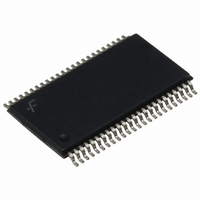
FIN1217MTDX Fairchild Semiconductor, FIN1217MTDX Datasheet - Page 9

FIN1217MTDX
Manufacturer Part Number
FIN1217MTDX
Description
IC SERIALIZER/DESERIAL 48-TSSOP
Manufacturer
Fairchild Semiconductor
Type
LVDS 21-Bit Serializer/Deserializerr
Datasheet
1.FIN1215MTDX.pdf
(20 pages)
Specifications of FIN1217MTDX
Function
Serializer/Deserializer
Data Rate
1.785Gbps
Input Type
LVTTL
Output Type
LVDS
Number Of Inputs
21
Number Of Outputs
3
Voltage - Supply
3 V ~ 3.6 V
Operating Temperature
-40°C ~ 85°C
Mounting Type
Surface Mount
Package / Case
48-TSSOP
Number Of Drivers
3
Number Of Receivers
21
Operating Supply Voltage
3.3 V
Maximum Operating Temperature
+ 150 C
Minimum Operating Temperature
- 65 C
Mounting Style
SMD/SMT
Supply Current
55 mA
Supply Voltage (max)
3.6 V
Supply Voltage (min)
3 V
Lead Free Status / RoHS Status
Lead free / RoHS Compliant
Other names
FIN1217MTDX
FIN1217MTDXTR
FIN1217MTDXTR
© 2003 Fairchild Semiconductor Corporation
FIN1215 / FIN1216 / FIN1217 • Rev. 1.0.3
Transmitter AC Electrical Characteristics
Transmitter Output Data Jitter (f=85 MHz, FIN1217 only)
Notes:
11. Outputs of all transmitters stay in 3-STATE until power reaches 2V. Clock and data output begins to toggle
12. This output data pulse position works for both transmitters with 21 TTL inputs, except the LVDS output bit
13. This jitter specification is based on the assumption that PLL has a reference clock with cycle-to-cycle input jitter
Symbol
t
t
t
t
t
t
t
t
TPPB0
TPPB1
TPPB2
TPPB3
TPPB4
TPPB5
TPPB6
TPLLS
t
JCC
10ms after V
mapping difference (see Figure 19). Figure 20 shows the skew between the first data bit and clock output. A
two-bit cycle delay is guaranteed when the MSB is output from transmitter.
of less than 2ns.
Transmitter Output Pulse Position of Bit 0
Transmitter Output Pulse Position of Bit 1
Transmitter Output Pulse Position of Bit 2
Transmitter Output Pulse Position of Bit 3
Transmitter Output Pulse Position of Bit 4
Transmitter Output Pulse Position of Bit 5
Transmitter Output Pulse Position of Bit 6
Transmitter Clock Out Jitter, Cycle-to cycle
Figure 23
Transmitter Phase Lock Loop Set Time
CC
reaches 3V and /PwrDn pin is above 1.5V.
Parameter
(13)
9
(12)
(Continued)
Figure 20
f=40MHz
f=65MHz
f=85MHz
FIN1217 only
Figure 15
a
=
Conditions
f
×
1
7
(12)
2a-0.2
3a-0.2
4a-0.2
5a-0.2
6a-0.2
a-0.2
Min.
-0.2
Typ.
350
210
110
2a
3a
4a
5a
6a
0
a
2a+0.2
3a+0.2
4a+0.2
5a+0.2
6a+0.2
a+0.2
Max.
10.0
370
230
150
0.2
www.fairchildsemi.com
Units
ms
ns
ns
ns
ns
ns
ns
ns
ps


