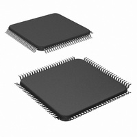
DS90CR486VSX/NOPB National Semiconductor, DS90CR486VSX/NOPB Datasheet - Page 11

DS90CR486VSX/NOPB
Manufacturer Part Number
DS90CR486VSX/NOPB
Description
IC DESERIALIZER 48BIT 100-TQFP
Manufacturer
National Semiconductor
Datasheet
1.DS90CR486VSNOPB.pdf
(18 pages)
Specifications of DS90CR486VSX/NOPB
Function
Deserializer
Data Rate
6.384Gbps
Input Type
LVDS
Output Type
LVTTL, LVCMOS
Number Of Inputs
8
Number Of Outputs
48
Voltage - Supply
3.14 V ~ 3.46 V
Operating Temperature
-10°C ~ 70°C
Mounting Type
Surface Mount
Package / Case
100-TQFP, 100-VQFP
For Use With
CLINK3V48BT-133 - BOARD EVAL FOR DS90CR485, 486
Lead Free Status / RoHS Status
Lead free / RoHS Compliant
Other names
DS90CR486VSX
Available stocks
Company
Part Number
Manufacturer
Quantity
Price
Company:
Part Number:
DS90CR486VSX/NOPB
Manufacturer:
Texas Instruments
Quantity:
10 000
RxINP
RxINM
RxOUT
RxCLKP
RxCLKM
RxCLKOUT
PLLSEL
PD
DESKEW
BAL
CON1
V
GND
PLLV
PLLGND
LVDSV
LVDSGND
NC
CC
DS90CR486 Pin Descriptions — Channel Link Receiver
Note 10: These receivers have input fail-safe bias circuitry to guarantee a stable receiver output for floating or terminated receiver inputs. Under these conditions
receiver inputs will be in a HIGH state. If a clock signal is present, outputs will all be HIGH; if the cable inter-connects are disconnected which results in floating/
terminated inputs, the outputs will remain in the last valid state. A floating/terminated clock input will result in a LOW clock output.
CC
Pin Name
CC
I/O
O
O
I
I
I
I
I
I
I
I
I
I
I
I
I
I
I
No.
48
8
8
1
1
1
1
1
1
1
1
6
8
1
2
2
3
6
Positive LVDS differential data inputs.
Negative LVDS differential data inputs.
LVCMOS/LVTTL level data outputs. In PowerDown (PD = Low) mode, receiver
outputs are forced to a Low state.
Positive LVDS differential clock input.
Negative LVDS differential clock input.
LVCMOS/LVTTL level clock output. The rising edge acts as data strobe.
Control input for PLL range select. This pin must be tied to V
tied to GND is reserved for future use.
Power Down pin. This pin must be tied to input level of 2.5V to Vcc for normal
operation. When de-asserted (low input) the receiver outputs are Low. Please
refer to the Applications Information on the back for more information.
This pin must be tied to logic High or Vcc for normal operation of Deskew function.
De-asserting a pulse of duration greater than 4 clock cycles will restart the deskew
initialization. Do NOT tie this pin to LOW. Please refer to the Applications
Information on the back for more information.
LVCMOS/LVTTL level input. This pin must be tied to logic High or Vcc to enable
DC Balance function(Figure 9). When tied low or left open, the DC Balance
function is disabled(Figure 8). Please refer to the Applications Information on the
back for more infomation.
Control Pin. This pin must be tied to logic High or Vcc.
Power supply pins for LVCMOS/LVTTL outputs and digital circuitry.
Ground pins for LVCMOS/LVTTL outputs and digital circuitry.
Power supply for PLL circuitry.
Ground pin for PLL circuitry.
Power supply pin for LVDS inputs.
Ground pins for LVDS inputs.
No Connect. Make NO Connection to these pins - leave open.
11
Description
CC
. No connect or
www.national.com


