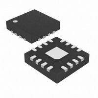
MAX9225ETE+T Maxim Integrated Products, MAX9225ETE+T Datasheet - Page 10

MAX9225ETE+T
Manufacturer Part Number
MAX9225ETE+T
Description
IC SERIALIZER LP 16-TQFN
Manufacturer
Maxim Integrated Products
Datasheet
1.MAX9226ETE.pdf
(15 pages)
Specifications of MAX9225ETE+T
Function
Serializer/Deserializer
Data Rate
200Mbps
Input Type
Parallel
Output Type
Parallel
Number Of Inputs
10
Number Of Outputs
1
Voltage - Supply
2.375 V ~ 3.465 V
Operating Temperature
-40°C ~ 85°C
Mounting Type
Surface Mount
Package / Case
16-TQFN Exposed Pad
Lead Free Status / RoHS Status
Lead free / RoHS Compliant
10-Bit, Low-Power, 10MHz-to-20MHz
Serializer and Deserializer Chipset
The parallel data input of the MAX9225 serializer is
latched on the rising edge of PCLKIN. Figure 3 shows
the serializer input timing.
The serial-data output of the MAX9226 deserializer is
valid on the rising edge of PCLKOUT. Figure 4 shows
the deserializer output timing.
Driving PWRDN low puts the MAX9225 in power-down
mode and sends a pulse to power down the MAX9226.
In power-down mode, the DLL is stopped, SDO+/SDO-
are high impedance to ground and differential, and the
LCDS link is weakly biased around (V
PWRDN and all inputs low, the combined MAX9225/
MAX9226 supply current is reduced to 3.5µA or less.
Driving PWRDN high starts DLL lock to PCLKIN and ini-
tiates a MAX9226 power-up sequence. The MAX9225
Figure 5. Multilevel LCDS Output Representation
10
______________________________________________________________________________________
NOTE: OH1 AND OH2 ARE OPPOSITE POLARITY.
LCDS SERIAL-DATA OUTPUT FOR EXAMPLE INPUT (SD0+/SDO-)
1
Applications Information
Power-Down and Power-Up
1
PCLK IN
DIN[9:0]
PARALLEL DATA INPUT
EXAMPLE
INPUT
DIN
PCLKIN Latch Edge
0
PCLKOUT Strobe
0
1
DD
1
- 0.8V). With
1
1
0
2
0
3
1
0
4
0
LCDS output is not driven until the DLL locks. 11,264
clock cycles are required for the power-up and link syn-
chronization before valid DIN can be latched. See
Figure 6 for an overall power-up and power-down tim-
ing diagram. For normal operation, PCLKIN must be
running and settled before driving PWRDN high.
If V
ground and differential.
The MAX9225/MAX9226 are designed to function nor-
mally in the event of a slight shift in ground potential.
However, the MAX9226 deserializer ground must be
within ±0.2V relative to the MAX9225 serializer ground
to maintain proper operation.
The MAX9226 parallel outputs are powered from V
which accepts a +1.71V to +3.465V supply, allowing
direct interface to inputs with 1.8V to 3.3V logic levels.
5
0
DD
1
MAX9226 Output Buffer Supply (V
= 0, the LCDS outputs are high impedance to
6
1
7
0
0
8
1
1
9
1
Ground-Shift Tolerance
1
OH1
OH2
DDO
DDO
)
,


