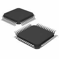
MAX9248ECM/V+T Maxim Integrated Products, MAX9248ECM/V+T Datasheet - Page 16

MAX9248ECM/V+T
Manufacturer Part Number
MAX9248ECM/V+T
Description
IC DESERIALIZER LVDS 48-LQFP
Manufacturer
Maxim Integrated Products
Datasheet
1.MAX9250ECMT.pdf
(20 pages)
Specifications of MAX9248ECM/V+T
Function
Deserializer
Data Rate
840Mbps
Input Type
LVDS
Output Type
LVTTL, LVCMOS
Number Of Inputs
1
Number Of Outputs
18
Voltage - Supply
3 V ~ 3.6 V
Operating Temperature
-40°C ~ 85°C
Mounting Type
Surface Mount
Package / Case
48-LQFP
Lead Free Status / RoHS Status
Lead free / RoHS Compliant
The MAX9248 single-ended data and clock outputs are
programmable for a variation of ±2% or ±4% around
the LVDS input clock frequency. The modulation rate of
the frequency variation is 32kHz for a 33MHz LVDS
clock input and scales linearly with the clock frequency
(see Table 4). The output spread is controlled through
the SS input (see Table 5). Driving SS high spreads all
data and clock outputs by ±4%, while pulling low
spreads ±2%.
27-Bit, 2.5MHz to 42MHz
DC-Balanced LVDS Deserializers
Table 4. Modulation Rate
Table 5. SS Function
Figure 17. Output Waveforms when Spread Amount is Changed
16
RGB_OUT[17:0]
CNTL_OUT8:0]
SS INPUT LEVEL
PCLK_OUT
______________________________________________________________________________________
LOCK
High
Low
SS
f
PCLK_IN
10
16
32
40
42
8
Spread-Spectrum Selection
±4% OR ±2% SPREAD
Data and clock output spread ±4%
relative to REFCLK
Data and clock output spread ±2%
relative to REFCLK
f
OUTPUT SPREAD
M
(kHz) = f
15.63
31.25
39.06
41.01
PCLK_IN
7.81
9.77
/ 1024
±4% OR ±2% SPREAD
t
ΔSSPLL
LOW
(32,800 x t
Any spread change causes a delay time of 32,000 x t
before output data is valid. When the spread amount is
changed from ±2% to ±4% or vice versa, the data out-
puts go low for one t
data outputs stay low, but are not valid when the
spread amount is changed.
The outputs of two MAX9250s can be bused to form a
2:1 mux with the outputs controlled by the output
enable. Wait 30ns between disabling one deserializer
(driving OUTEN low) and enabling the second one (dri-
ving OUTEN high) to avoid contention of the bused out-
puts. OUTEN controls all outputs except LOCK.
The MAX9248/MAX9250 have a selectable rising or
falling output latch edge through a logic setting on R/F.
Driving R/F high selects the rising output latch edge,
which latches the parallel output data into the next chip
on the rising edge of PCLK_OUT. Driving R/F low
selects the falling output latch edge, which latches the
parallel output data into the next chip on the falling
edge of PCLK_OUT. The MAX9248/MAX9250 output-
latch-edge polarity does not need to match the
MAX9247 serializer input-latch-edge polarity. Select the
latch-edge polarity required by the chip being driven
by the MAX9248/MAX9250.
Rising or Falling Output Latch Edge (R/ F )
T
)
Output Enable (OUTEN) and
ΔSSPLL
delay (see Figure 17). The
Busing Outputs
T


