MAX9247ECM+ Maxim Integrated Products, MAX9247ECM+ Datasheet - Page 10
MAX9247ECM+
Manufacturer Part Number
MAX9247ECM+
Description
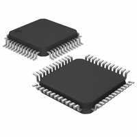
IC SERIALIZER LVDS 48-LQFP
Manufacturer
Maxim Integrated Products
Datasheet
1.MAX9247ECMT.pdf
(17 pages)
Specifications of MAX9247ECM+
Function
Serializer
Data Rate
840Mbps
Input Type
Serial
Output Type
LVDS
Number Of Inputs
18
Number Of Outputs
1
Voltage - Supply
3 V ~ 3.6 V
Operating Temperature
-40°C ~ 85°C
Mounting Type
Surface Mount
Package / Case
48-LQFP
Lead Free Status / RoHS Status
Lead free / RoHS Compliant


27-Bit, 2.5MHz-to-42MHz
DC-Balanced LVDS Serializer
Figure 8. Peak-to-Peak Output Offset Voltage
The MAX9247 DC-balanced serializer operates at a
2.5MHz-to-42MHz parallel clock frequency, serializing
18 bits of parallel video data RGB_IN[17:0] when the
data-enable input DE_IN is high, or 9 bits of parallel
control data CNTL_IN[8:0] when DE_IN is low. The
RGB video input data are encoded using 2 overhead
bits, EN0 and EN1, resulting in a serial word length of
20 bits (see Table 1). Control inputs are mapped to 19
bits and encoded with 1 overhead bit, EN0, also result-
ing in a 20-bit serial word. Encoding reduces EMI and
Table 1. Serial Video Phase Word Format
Bit 0 is the LSB and is serialized first. EN[1:0] are encoding bits. S[17:0] are encoded symbols.
Table 2. Serial Control Phase Word Format
Bit 0 is the LSB and is serialized first. C[8:0] are the control inputs.
10
EN0
E N 0
0
0
((OUT+) + (OUT-))/2
______________________________________________________________________________________
EN1
C0
1
1
OUT+
OUT-
C0
S0
2
2
C0
S1
3
3
Detailed Description
C1
S2
4
4
C1
S3
5
5
C1
S4
6
6
V
OS(P-P)
C2
S5
7
7
C2
S6
8
8
C2
S7
9
9
C3
10
S8
10
maintains DC balance across the serial cable. Two
transition words, which contain a unique bit sequence,
are inserted at the transition boundaries of video-to-
control and control-to-video phases.
Control data inputs C0 to C4 are mapped to 3 bits each
in the serial control word (see Table 2). At the deserial-
izer, 2 or 3 bits at the same state determine the state of
the recovered bit, providing single-bit-error tolerance
for C0 to C4. Control data that may be visible if an error
occurs, such as VSYNC and HSYNC, can be connect-
ed to these inputs. Control data inputs C5 to C8 are
mapped to 1 bit each.
C3
S9
11
11
S10
C3
12
12
V
S11
C4
OS(P-P)
13
13
S12
C4
14
14
S13
C4
15
15
S14
C5
16
16
S15
C6
17
17
S16
C7
18
18
S17
C8
19
19
Related parts for MAX9247ECM+
Image
Part Number
Description
Manufacturer
Datasheet
Request
R

Part Number:
Description:
Max9247 27-bit, 2.5mhz-to-42mhz Dc-balanced Lvds Serializer
Manufacturer:
Maxim Integrated Products, Inc.
Datasheet:

Part Number:
Description:
MAX7528KCWPMaxim Integrated Products [CMOS Dual 8-Bit Buffered Multiplying DACs]
Manufacturer:
Maxim Integrated Products
Datasheet:
Part Number:
Description:
Single +5V, fully integrated, 1.25Gbps laser diode driver.
Manufacturer:
Maxim Integrated Products
Datasheet:
Part Number:
Description:
Single +5V, fully integrated, 155Mbps laser diode driver.
Manufacturer:
Maxim Integrated Products
Datasheet:
Part Number:
Description:
VRD11/VRD10, K8 Rev F 2/3/4-Phase PWM Controllers with Integrated Dual MOSFET Drivers
Manufacturer:
Maxim Integrated Products
Datasheet:
Part Number:
Description:
Highly Integrated Level 2 SMBus Battery Chargers
Manufacturer:
Maxim Integrated Products
Datasheet:
Part Number:
Description:
Current Monitor and Accumulator with Integrated Sense Resistor; ; Temperature Range: -40°C to +85°C
Manufacturer:
Maxim Integrated Products
Part Number:
Description:
TSSOP 14/A�/RS-485 Transceivers with Integrated 100O/120O Termination Resis
Manufacturer:
Maxim Integrated Products
Part Number:
Description:
TSSOP 14/A�/RS-485 Transceivers with Integrated 100O/120O Termination Resis
Manufacturer:
Maxim Integrated Products
Part Number:
Description:
QFN 16/A�/AC-DC and DC-DC Peak-Current-Mode Converters with Integrated Step
Manufacturer:
Maxim Integrated Products
Part Number:
Description:
TDFN/A/65V, 1A, 600KHZ, SYNCHRONOUS STEP-DOWN REGULATOR WITH INTEGRATED SWI
Manufacturer:
Maxim Integrated Products
Part Number:
Description:
Integrated Temperature Controller f
Manufacturer:
Maxim Integrated Products
Part Number:
Description:
SOT23-6/I�/45MHz to 650MHz, Integrated IF VCOs with Differential Output
Manufacturer:
Maxim Integrated Products
Part Number:
Description:
SOT23-6/I�/45MHz to 650MHz, Integrated IF VCOs with Differential Output
Manufacturer:
Maxim Integrated Products
Part Number:
Description:
EVALUATION KIT/2.4GHZ TO 2.5GHZ 802.11G/B RF TRANSCEIVER WITH INTEGRATED PA
Manufacturer:
Maxim Integrated Products