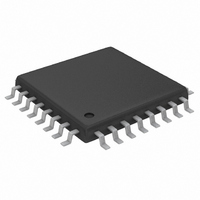
MAX3693ECJ Maxim Integrated Products, MAX3693ECJ Datasheet - Page 4

MAX3693ECJ
Manufacturer Part Number
MAX3693ECJ
Description
IC SERIALIZR 622MBPS LVDS 32TQFP
Manufacturer
Maxim Integrated Products
Datasheet
1.MAX3693ECJ.pdf
(8 pages)
Specifications of MAX3693ECJ
Function
Serializer
Data Rate
622Mbps
Input Type
LVDS
Output Type
PECL
Number Of Inputs
4
Number Of Outputs
1
Voltage - Supply
3 V ~ 3.6 V
Operating Temperature
-40°C ~ 85°C
Mounting Type
Surface Mount
Package / Case
32-LQFP
Lead Free Status / RoHS Status
Contains lead / RoHS non-compliant
Available stocks
Company
Part Number
Manufacturer
Quantity
Price
Part Number:
MAX3693ECJ
Manufacturer:
MAXIM/美信
Quantity:
20 000
Company:
Part Number:
MAX3693ECJ+
Manufacturer:
AKM
Quantity:
137
Company:
Part Number:
MAX3693ECJ+
Manufacturer:
Maxim Integrated
Quantity:
10 000
Company:
Part Number:
MAX3693ECJ+T
Manufacturer:
Maxim Integrated
Quantity:
10 000
+3.3V, 622Mbps, SDH/SONET 4:1 Serializer
with Clock Synthesis and LVDS Inputs
4
(V
9, 17, 18, 19,
12, 13, 16,
CC
24, 25, 32
21, 28, 29
1, 3, 5, 7
2, 4, 6, 8
_______________________________________________________________________________________
PIN
= +3.3V, differential LVDS loads = 100Ω ±1%, PECL loads = 50Ω ±1% to (V
10
11
14
15
20
22
23
26
27
30
31
57mV/
0.536V
1.1V
div
PD0+ to PD3+
PD0- to PD3-
SERIAL-DATA OUTPUT EYE DIAGRAM
PCLKO+
PCLKO-
PCLKI+
RCLK+
CKSET
PCLKI-
NAME
RCLK-
GND
FIL+
SD+
V
SD-
FIL-
CC
200ps/div
Noninverting LVDS Parallel Data Inputs. Data is clocked in on the PCLKI signal’s positive transition.
Inverting LVDS Parallel Data Inputs. Data is clocked in on the PCLKI signal’s positive transition.
Ground
Inverting LVDS Parallel-Clock Output. Use positive transition of PCLKO to clock the overhead man-
agement circuit.
Noninverting LVDS Parallel-Clock Output. Use positive transition of PCLKO to clock the overhead
management circuit.
+3.3V Supply Voltage
Inverting PECL Serial-Data Output
Noninverting PECL Serial-Data Output
Reference Clock Rate Programming Pin.
CKSET = V
CKSET = Open: Reference Clock Rate = 77.76MHz
CKSET = 20kΩ to GND: Reference Clock Rate = 51.84MHz
CKSET = GND Reference Clock Rate = 38.88MHz
Filter Capacitor Input. See Typical Operating Circuit for external-component connections.
Filter Capacitor Input. See Typical Operating Circuit for external-component connections.
Noninverting LVDS Reference Clock Input. Connect an LVDS-compatible crystal reference clock to
the RCLK inputs.
Inverting LVDS Reference Clock Input. Connect an LVDS-compatible crystal reference clock to the
RCLK inputs.
Noninverting LVDS Parallel Clock Input. Connect the incoming parallel-data-clock signal to the
PCLKI inputs. Note that data is updated on the positive transition of the PCLKI signal.
Inverting LVDS Parallel Clock Input. Connect the incoming parallel-data-clock signal to the PCLKI
inputs. Note that data is updated on the positive transition of the PCLKI signal.
CC
: Reference Clock Rate = 155.52MHz
Typical Operating Characteristics (continued)
1.0042V
0.904V
10mV/
FUNCTION
div
CC
Mean 25.22ns
RMS ∆ 4.073ps
PkPk 32.6ps
- 2V), T
SERIAL-DATA OUTPUT JITTER
A
= +25°C, unless otherwise noted.)
10ps/div
f
RCLK
µ ±1 σ 70.373%
µ ±2 σ 95.357%
µ ±3 σ 99.759%
= 155.52MHz
Pin Description


