PI3PCIE2612-AZFE Pericom Semiconductor, PI3PCIE2612-AZFE Datasheet
PI3PCIE2612-AZFE
Specifications of PI3PCIE2612-AZFE
Available stocks


Related parts for PI3PCIE2612-AZFE

PI3PCIE2612-AZFE Summary of contents
Page 1
... High Bandwidth, 6-Differential Channel 1:2 DP/PCIe Gen2 Display Mux, ATX Pinout Description Pericom Semiconductor’s PI3PCIE2612-A one to two Mux/ Demux is targeted for next generation systems that combine PCI- Express gen-II signals with Display Port Signals. Application Routing DP and PCIExpress Gen1 or Gen2 signals with low signal attenuation ...
Page 2
... IN_1-, when SEL = 1. O Analog “pass through” output#1 corresponding to IN_2+ and IN_2-, when SEL = 1. O Analog “pass through” output#1 corresponding to IN_3+ and IN_3-, when SEL = 1. 2 PI3PCIE2612-A High Bandwidth, 6-Differential Channel Dx HPD DP Path will support 2.7 Gbps AUX PCIe ...
Page 3
... Differential input from PCIE connector or device. Rx0- makes a differential pair with Rx0+. Rx0- is passed through to the OUT- pin when SEL = 0. I Differential input from PCIE connector or device. Rx1+ makes a differential pair with Rx1-. Rx1+ is passed through to the X+ pin when SEL = 0. (Continued) 3 PI3PCIE2612-A High Bandwidth, 6-Differential Channel PS8925D 07/31/08 ...
Page 4
... X+: Analog “pass through” output corresponding to Rx1 analog “pass-through” output corresponding to the Rx1- input. The path from Rx1 must be matched with the path from Rx1+ to X+. X+ and X- form a differential pair when the pass-through mux mode is selected. 4 PI3PCIE2612-A High Bandwidth, 6-Differential Channel PS8925D 07/31/08 ...
Page 5
... 25°C ambient and maximum loading. 5 PI3PCIE2612-A High Bandwidth, 6-Differential Channel Note: Stresses greater than those listed under MAX I MUM RAT INGS may cause permanent damage to the de vice. This is a stress rating only and func tion tion of the device at these or any other conditions above those indicated in the operational sections of this spec i fi ...
Page 6
... See "Test Circuit for X XY Electrical Chatacteristics" ±, T ±, See "Test Circuit for X XY Electrical Chatacteristics" See "Test Circuit for Electrical Chatacteristics" See "Test Circuit for Electrical Chatacteristics" 6 PI3PCIE2612-A (1) Min. Typ. Max. Units -1.5 -2.0 -5.0 -9.0 -23.0 -20.0 dB -14.0 -8.0 -4 ...
Page 7
... DP/PCIe Gen2 Display Mux, ATX Pinout Differential Insertion Loss Differential Return Loss 7 PI3PCIE2612-A High Bandwidth, 6-Differential Channel PS8925D 07/31/08 ...
Page 8
... High Bandwidth, 6-Differential Channel 1:2 DP/PCIe Gen2 Display Mux, ATX Pinout Off Isolation Crosstalk 8 PI3PCIE2612-A PS8925D 07/31/08 ...
Page 9
... High Bandwidth, 6-Differential Channel 1:2 DP/PCIe Gen2 Display Mux, ATX Pinout Tx Eye Diagram, 5.0 Gbps Dx Eye Diagram, 2.7 Gbps 9 PI3PCIE2612-A PS8925D 07/31/08 ...
Page 10
... High Bandwidth, 6-Differential Channel 1:2 DP/PCIe Gen2 Display Mux, ATX Pinout Test Circuit Test Circuit Test Circuit 10 PI3PCIE2612-A PS8925D 07/31/08 ...
Page 11
... Prop Delay 4pF 200-ohm the Pulse Generator OUT SEL PZL t PLZ V V DD/2 t PHZ t PZH V V DD/2 Voltage Waveforms Enable and Disable Times 11 PI3PCIE2612-A High Bandwidth, 6-Differential Channel Switch , PZL , t GND PZH Open = 50Ω, t ≤ 2.5ns, t ≤ 2.5ns 0.15V – 0.15V OH ...
Page 12
... GHz); ≤ - 2.8 GHz; ≤ GHz; ≤ 7.5 GHz. -32 dB max up to 2.5 GHz max up to 5.0 GHz; -20 dB max up to 7.5 GHz; ≤ - GHz; 12 PI3PCIE2612-A Units Comments Ps Defi ned by Gen2 spec. V VRX-DIFFp-p = 2*|VRX VRX-D-|. Applies to IN_D and RX_IN signals. ...
Page 13
... GHz; ≤ 7.5 GHz. -32 dB max up to 2.5 GHz; dB -26 dB max up to 5.0 GHz; -20 dB max up to 7.5 GHz; ≤ - GHz PI3PCIE2612-A Comments Rx DC Differential Mode impedance. Required IN_D+ as well as IN_D- DC imped- ance (50Ω +/- 20% tol- erance). Includes mux resistance. Intended to limit pow- er-up stress on PCIE output buffers ...
Page 14
... Min Nom Max Units 1.3K 1.5k 2. PI3PCIE2612-A Comments Normal Tbit at 2.7Gb/ s=370ps. 333ps=370ps- 10% VRX-DIFFp-p = 2*|VRX-D+ - VRX-D- |. Applies to IN_D and RX_IN signals. Jitter budget for high- speed signals as they pass through the display mux. 7.4ps = 0.02 Tbit at 2.7Gb/s For example, ≥-1 1.35 GHz For example, ≥ ...
Page 15
... GHz (for example, ≥- 7.5 GHz); Refer to Figure 1. ≤ - 2.8 GHz; ≤ GHz; ≤ 7.5 GHz. Refer to Figure max -32 dB max up to 2.5 GHz; -26 dB max up to 5.0 GHz; -20 dB max up to 7.5 GHz; See Figure 3. ≤ - GHz; 15 PI3PCIE2612-A PS8925D 07/31/08 ...
Page 16
... Figure 1: Illustration of differential insertion loss requirement -10 -15 -20 -25 - Figure 2: Illustration of differential return loss requirement. 08-0145 High Bandwidth, 6-Differential Channel 1:2 DP/PCIe Gen2 Display Mux, ATX Pinout Frequency, GHz Frequency, GHz 16 PI3PCIE2612-A SDD21 Zref=100 Ohms SDD11 Zref=100 Ohms PS8925D 07/31/08 ...
Page 17
... SMA to the trace. The impedance range of the SMA seen from a TDR with rise time should be within 50+/-7 ohms. 08-0145 High Bandwidth, 6-Differential Channel 1:2 DP/PCIe Gen2 Display Mux, ATX Pinout Frequency, GHz 17 PI3PCIE2612-A SDD21 Zref=85 Ohms PS8925D 07/31/08 ...
Page 18
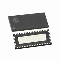
... Packaging Mechanical: 56-Contact TQFN (ZFE) Ordering Information Ordering Code PI3PCIE2612-AZFE Notes: • Thermal characteristics can be found on the company web site at www.pericom.com/packaging/ • "E" denotes Pb-free and Green • Adding an "X" at the end of the ordering code denotes tape and reel packaging Pericom Semiconductor Corporation • 1-800-435-2336 • www.pericom.com ...