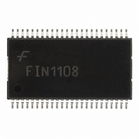
FIN1108MTDX Fairchild Semiconductor, FIN1108MTDX Datasheet - Page 6

FIN1108MTDX
Manufacturer Part Number
FIN1108MTDX
Description
IC REPEATER 8PORT LVDS 48-TSSOP
Manufacturer
Fairchild Semiconductor
Type
Repeaterr
Datasheet
1.FIN1108MTD.pdf
(9 pages)
Specifications of FIN1108MTDX
Tx/rx Type
LVDS
Delay Time
1.75ns
Capacitance - Input
3pF
Voltage - Supply
3 V ~ 3.6 V
Current - Supply
80mA
Mounting Type
Surface Mount
Package / Case
48-TSSOP
Supply Voltage (max)
3.6 V
Supply Voltage (min)
3 V
Maximum Operating Temperature
+ 150 C
Mounting Style
SMD/SMT
Data Rate
800 Mbps
Interface
EIA/TIA-644-A
Minimum Operating Temperature
- 65 C
Supply Current
80 mA
Lead Free Status / RoHS Status
Lead free / RoHS Compliant
Other names
FIN1108MTDX
FIN1108MTDXTR
FIN1108MTDXTR
Available stocks
Company
Part Number
Manufacturer
Quantity
Price
Company:
Part Number:
FIN1108MTDX
Manufacturer:
FSC
Quantity:
1 579
Part Number:
FIN1108MTDX
Manufacturer:
ON/ه®‰و£®ç¾ژ
Quantity:
20 000
© 2002 Fairchild Semiconductor Corporation
FIN1108 • Rev. 1.0.4
AC Electrical Characteristics
Typical values are at T
Notes:
1.
2.
3.
4.
Symbol
t
t
t
t
t
t
t
t
t
t
SK(LH)
SK(HL)
SK(PP)
t
t
f
t
are switching in the same direction.
t
devices switching in the same direction (either LOW-to-HIGH or HIGH-to-LOW) when both devices operate with
the same supply voltage, same temperature, and have identical test circuits.
Passing criteria for maximum frequency is the output V
with all channels switching.
Output loading is transmission-line environment only; C
PLHD
PHLD
SK(P)
PZHD
PHZD
TLHD
THLD
PZLD
PLZD
MAX
t
t
SK(LH)
SK(PP)
DJ
RJ
, t
is the magnitude of the difference in propagation delay times between any specified terminals of two
SK(HL)
Differential Output
Propagation Delay
LOW-to-HIGH
Differential Output
Propagation Delay
HIGH-to-LOW
Differential Output Rise
Time (20% to 80%)
Differential Output Fall
Time (80% to 20%)
Pulse Skew
|t
Channel-to-Channel
Skew
Part-to-Part Skew
Maximum Frequency
Differential Output
Enable Time from
Z to HIGH
Differential Output
Enable Time from
Z to LOW
Differential Output
Disable Time from
HIGH to Z
Differential Output
Disable Time from
LOW to Z
LVDS Data Jitter,
Deterministic
LVDS Clock Jitter,
Random (RMS)
PLH
is the skew between specified outputs of a single device when the outputs have identical loads and
- t
(1)
Parameter
PHL
A
=25°C with V
|
(2)
(3)(4)
CC
=3.3V.
R
V
V
Duty Cycle=50%
Figure 3
R
Figure 4, Figure 5
V
V
V
V
ID
IC
ID
IC
ID
IC
L
L
=100Ω, C
=100Ω, C
=200mV to 450mV,
= V
=300mV, PRBS=2
=1.2V at 800Mbps
=300mV
=1.2V at 400Mbps
ID
/2 to V
Conditions
L
L
=5pF
=5pF
CC
6
– (V
OD
L
is <1pF of stray test fixture capacitance.
>250mV and the duty cycle is better than 45% / 55%
ID
23
/2)
-1,
Min.
0.75
0.75
0.29
0.29
400
Typ.
>630
1.10
1.10
0.40
0.40
0.02
0.02
0.02
3.0
3.1
2.2
2.5
1.9
80
Max.
1.75
1.75
0.58
0.58
0.20
0.15
0.15
135
0.5
5.0
5.0
5.0
5.0
3.5
www.fairchildsemi.com
Units
MHz
ns
ns
ns
ns
ns
ns
ns
ns
ns
ns
ns
ps
ps


