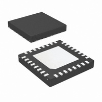
DS90LV804TSQ/NOPB National Semiconductor, DS90LV804TSQ/NOPB Datasheet - Page 3

DS90LV804TSQ/NOPB
Manufacturer Part Number
DS90LV804TSQ/NOPB
Description
IC BUFF REPEATER LVDS 4CH 32LLP
Manufacturer
National Semiconductor
Type
Bufferr
Datasheet
1.DS90LV804TSQXNOPB.pdf
(10 pages)
Specifications of DS90LV804TSQ/NOPB
Tx/rx Type
LVDS
Delay Time
3.2ns
Capacitance - Input
3.5pF
Voltage - Supply
3.15 V ~ 3.45 V
Current - Supply
140mA
Mounting Type
Surface Mount
Package / Case
32-LLP
Lead Free Status / RoHS Status
Lead free / RoHS Compliant
Other names
DS90LV804TSQ
DS90LV804TSQTR
DS90LV804TSQTR
Available stocks
Company
Part Number
Manufacturer
Quantity
Price
Company:
Part Number:
DS90LV804TSQ/NOPB
Manufacturer:
FREE
Quantity:
840
DIFFERENTIAL INPUTS
IN0+
IN0−
IN1+
IN1−
IN2+
IN2−
IN3+
IN3−
DIFFERENTIAL OUTPUTS
OUT0+
OUT0−
OUT1+
OUT1−
OUT2+
OUT2−
OUT3+
OUT3-
DIGITAL CONTROL INTERFACE
EN
POWER
V
GND
N/C
DD
Name
Pin Descriptions
Note 1: Note that for the LLP package the GND is connected thru the DAP on the back side of the LLP package in addition to grounding actual pins on the
package as listed.
Note 2: The LVDS outputs do not support a multidrop (BLVDS) environment. The LVDS output characteristics of the DS90LV804 device have been optimized
for point-to-point backplane and cable applications.
Pin
3, 4, 6, 7, 19, 20, 21, 22
1, 2, 5, 17, 18
LLP Pin
Number
(Note 1)
23, 24
10
11
12
13
14
15
16
32
31
30
29
28
27
26
25
9
8
I/O, Type
O, LVDS Channel 0 inverting and non-inverting differential outputs. (Note 2)
O, LVDS Channel 1 inverting and non-inverting differential outputs. (Note 2)
O, LVDS Channel 2 inverting and non-inverting differential outputs. (Note 2)
O, LVDS Channel 3 inverting and non-inverting differential outputs. (Note 2)
I, LVTTL Enable pin. When EN is LOW, the driver is disabled and the LVDS outputs are in TRI-
I, Power V
I, Power Ground reference for LVDS and CMOS circuitry. For the LLP package, the DAP is
I, LVDS Channel 0 inverting and non-inverting differential inputs.
I, LVDS Channel 1 inverting and non-inverting differential inputs.
I, LVDS Channel 2 inverting and non-inverting differential inputs.
I, LVDS Channel 3 inverting and non-inverting differential inputs.
STATE. When EN is HIGH, the driver is enabled. LVCMOS/LVTTL level input.
used as the primary GND connection to the device. The DAP is the exposed metal
contact at the bottom of the LLP-32 package. It should be connected to the ground
plane with at least 4 vias for optimal AC and thermal performance. The pin numbers
listed should also be tied to ground for proper biasing.
No Connect
DD
= 3.3V, ±5%
3
Description
www.national.com


