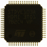
STDVE103ABTR STMicroelectronics, STDVE103ABTR Datasheet - Page 38

STDVE103ABTR
Manufacturer Part Number
STDVE103ABTR
Description
IC EQUALIZER TMDS/HDMI 64-TQFP
Manufacturer
STMicroelectronics
Datasheet
1.STDVE103ABTR.pdf
(44 pages)
Specifications of STDVE103ABTR
Applications
TV
Interface
I²C
Voltage - Supply
3.3V, 5V
Package / Case
64-TQFP, 64-VQFP
Mounting Type
Surface Mount
Lead Free Status / RoHS Status
Lead free / RoHS Compliant
Other names
497-8384-2
Available stocks
Company
Part Number
Manufacturer
Quantity
Price
Company:
Part Number:
STDVE103ABTR
Manufacturer:
TI
Quantity:
9 925
Company:
Part Number:
STDVE103ABTR
Manufacturer:
STMicroelectronics
Quantity:
10 000
Part Number:
STDVE103ABTR
Manufacturer:
ST
Quantity:
20 000
Application information
6
6.1
6.2
6.3
38/44
Application information
Power supply sequencing
Proper power-supply sequencing is advised for all CMOS devices. It is recommended to
always apply V
Power supply requirements
Bypass each of the V
device as possible, with the smaller-valued capacitor as close to the V
possible.
All V
from each V
variation can only be ±5% as per the HDMI specifications.
The maximum tolerable noise ripple on 3.3 V supply must be within a specified limit.
Differential traces
The high-speed TMDS inputs are the most critical parts for the device. There are several
considerations to minimize discontinuities on these transmission lines between the
connectors and the device.
(a) Maintain 100-Ω differential transmission line impedance into and out of the STDVE103A.
(b) Keep an uninterrupted ground plane below the high-speed I/Os.
(c) Keep the ground-path vias to the device as close as possible to allow the shortest return
current path.
(d) Layout of the TMDS differential inputs should be with the shortest stubs from the
connectors.
Output trace characteristics affect the performance of the STDVE103A. Use controlled
impedance traces to match trace impedance to both the transmission medium impedance
and termination resistor. Run the differential traces close together to minimize the effects of
the noise. Reduce skew by matching the electrical length of the traces. Avoid discontinuities
in the differential trace layout. Avoid 90 degree turns and minimize the number of vias to
further prevent impedance discontinuities.
CC
pins can be tied to a single 3.3 V power source. A 0.01 μF capacitor is connected
CC
CC
pin directly to ground to filter supply noise. The maximum power supply
before applying any signals to the input/output or control pins.
CC
pins with 0.1 μF and 1 nF capacitors in parallel as close to the
Doc ID 14911 Rev 4
CC
pin of the device as
STDVE103A


