TSI310A-133CE IDT, Integrated Device Technology Inc, TSI310A-133CE Datasheet
TSI310A-133CE
Manufacturer Part Number
TSI310A-133CE
Description
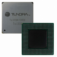
IC PCI-PCI BRIDGE 64BIT 304BGA
Manufacturer
IDT, Integrated Device Technology Inc
Series
Tsi310&Trade;r
Datasheet
1.TSI310A-133CE.pdf
(2 pages)
Specifications of TSI310A-133CE
Applications
PCI, PCI-X
Interface
PCI
Voltage - Supply
3.3V
Package / Case
304-CBGA
Mounting Type
Surface Mount
Lead Free Status / RoHS Status
Lead free / RoHS Compliant
Other names
800-1904
Available stocks
Company
Part Number
Manufacturer
Quantity
Price
Company:

Part Number:
TSI310A-133CE
Manufacturer:
SKHYNIX
Quantity:
28
Company:
Part Number:
TSI310A-133CE
Manufacturer:
IDT, Integrated Device Technology Inc
Quantity:
10 000
Company:
Part Number:
TSI310A-133CEY
Manufacturer:
MIC
Quantity:
11
Company:
Part Number:
TSI310A-133CEY
Manufacturer:
IDT, Integrated Device Technology Inc
Quantity:
10 000


Device Overview
The IDT Tsi310 is a 64-bit PCI-X bus bridge that operates at speeds up
to 133 MHz, and supports transfer rates up to 1 GBps. The PCI-X
protocol is backward compatible with the PCI 2.2 bus standard ensuring
that legacy PCI-based systems are portable to the faster PCI-X environ-
ment.
The Tsi310 connects two electrically separate PCI-X bus domains,
allowing concurrent operations on both buses. This results in optimal
use of the buses in various system configurations, and enables hierar-
chical expansion of I/O bus structures. The device also supports config-
urations of PCI or PCI-X mode on either bus, and in any combination.
In addition, the Tsi310 provides extensive buffering and prefetching
mechanisms for efficient data transfer between two buses, facilitating
multi-threaded operation and high system throughput.
Block Diagram
PCI-X Interfaces
The Tsi310 has two identical PCI-X Interfaces that each handle PCI and
PCI-X transactions for its respective bus, and, depending on the type of
transaction, can act as either a bus master or a bus slave. These inter-
faces transfer data and control information flowing to and from the
blocks shown in the figure.
The Tsi310 uses the 3.3V signaling environment. It employs two phase-
locked loops (PLLs), one for the primary clock domain and one for the
secondary clock domain. The PLL for each domain is used when the
bus is operating in PCI-X mode. In PCI mode, the PLL is bypassed to
2008 Integrated Device Technology, Inc.
Clock PLL
Interface
Primary
Master
PCI-X
JTAG
Slave
Bus
Bus
Read Queue
Read Queue
Burst Read
Burst Read
Compare
Compare
4 Kbytes
8 entries
4 Kbytes
8 entries
Queue
Queue
Buffer
Buffer
Logic
Logic
Data/Control Unit
Data/Control Unit
Clocking & Reset
Posted Write
Posted Write
PW Queue
PW Queue
8 entries
8 entries
1 Kbyte
Address
1 Kbyte
Address
IDT and the IDT logo are registered trademarks of Integrated Device Technology, Inc.
Decode
Decode
Buffer
Buffer
®
Phase Buffer
Phase Buffer
Single Data
Single Data
4 Bytes
Control
4 Bytes
Control
Logic
Logic
Tsi310
Product Brief
Bus Arbiter
Secondary
Secondary
Clock PLL
Interface
Master
80B6000_BK001_03
PCI-X
Slave
Bus
Bus
1 of 2
™
allow full frequency range as required by the bus architecture. The two
bus clocks may be run synchronously or asynchronously, and a spread-
spectrum clock input is supported for either or both interfaces.
Memory Buffer Architecture
The Tsi310 memory buffer architecture has the following features (see
Data/Control unit in the Block Diagram):
Transaction Forwarding
The Tsi310 includes one data/control unit for downstream transactions
and one for upstream transactions. Each of these identical units
contains separate buffers for burst read, posted write, and single data
phase operations. Also included in these blocks are write queues, queue
compare logic, address decoding upstream for forwarding, control logic,
and other control functions. The clocking and reset control unit manages
these common device functions.
The device has I/O and Memory Base Address registers and Prefetch-
able Memory Base Address registers for downstream forwarding, as
well as inverse decoding for upstream forwarding, VGA-compatible
addressing, and palette snooping for upstream transactions. The Tsi310
uses a flat addressing model and supports 64-bit addressing and dual
address cycles.
The Tsi310 responds as a medium-speed device on both PCI-X Inter-
faces, and supports fast, back-to-back transactions as a bus slave.
PCI Bus Arbitration
The Tsi310 uses an arbiter for the secondary bus, which can be disabled
if an external arbiter is employed. When enabled, bus arbitration is
provided for the Tsi310 and up to six external masters. Each bus master
can be assigned high or low priority, or be masked off.
Opaque Addressing (Optional)
The Tsi310 has an optional feature that can define an opaque (unde-
coded) memory address region to facilitate applications with embedded
processors.
• Two 4-Kbyte burst read buffers that support up to eight
• Two 1-Kbyte posted write buffers that support up to eight
• Two 4-Byte single data phase buffers that support transaction
133-MHz PCI-X Bridge
concurrent, upstream and downstream transactions
concurrent, upstream and downstream transactions
forwarding in either direction
September 4, 2009
Related parts for TSI310A-133CE
Image
Part Number
Description
Manufacturer
Datasheet
Request
R

Part Number:
Description:
IC PCI-PCI BRIDGE 64BIT 304BGA
Manufacturer:
IDT, Integrated Device Technology Inc
Datasheet:

Part Number:
Description:
TRANSLATION DEVICE DPI 80-PQFP
Manufacturer:
IDT, Integrated Device Technology Inc
Datasheet:
Part Number:
Description:
IDT PART
Manufacturer:
IDT, Integrated Device Technology Inc
Datasheet:
Part Number:
Description:
IC LIU T1/E1/J1 OCTAL 256PBGA
Manufacturer:
IDT, Integrated Device Technology Inc
Datasheet:

Part Number:
Description:
IC FREQ TIMING GENERATOR 28TSSOP
Manufacturer:
IDT, Integrated Device Technology Inc
Datasheet:
Part Number:
Description:
IC CLK DVR PLL 1:10 40VFQFPN
Manufacturer:
IDT, Integrated Device Technology Inc
Datasheet:
Part Number:
Description:
IC CLK FANOUT BUFFER 1:18 32LQFP
Manufacturer:
IDT, Integrated Device Technology Inc
Datasheet:
Part Number:
Description:
IC CLK FANOUT BUFFER 1:18 32LQFP
Manufacturer:
IDT, Integrated Device Technology Inc
Datasheet:
Part Number:
Description:
IC CK505 VREG/RES 56TSSOP
Manufacturer:
IDT, Integrated Device Technology Inc
Datasheet:

Part Number:
Description:
IC SDRAM CLK DVR 1:10 48-TSSOP
Manufacturer:
IDT, Integrated Device Technology Inc
Datasheet:

Part Number:
Description:
IC CLK DVR PLL 1:10 48TSSOP
Manufacturer:
IDT, Integrated Device Technology Inc
Datasheet:
Part Number:
Description:
IC FLEXPC CLK PROGR P4 56-TSSOP
Manufacturer:
IDT, Integrated Device Technology Inc
Datasheet:
Part Number:
Description:
IC FLEXPC CLK PROGR P4 56-TSSOP
Manufacturer:
IDT, Integrated Device Technology Inc
Datasheet:
Part Number:
Description:
IC FLEXPC CLK PROGR P4 56-SSOP
Manufacturer:
IDT, Integrated Device Technology Inc
Datasheet:

Part Number:
Description:
IC PLL CLK DRIVER 2.5V 28-TSSOP
Manufacturer:
IDT, Integrated Device Technology Inc
Datasheet:
TSI310A-133CE Summary of contents
Page 1
Device Overview The IDT Tsi310 is a 64-bit PCI-X bus bridge that operates at speeds up to 133 MHz, and supports transfer rates GBps. The PCI-X protocol is backward compatible with the PCI 2.2 bus standard ...
Page 2
Tsi310 Product Brief Features • Industry-standard 64-bit, 133-MHz PCI-X bridge chip • Full PCI 2.2 backward compatibility • Allows concurrent primary and secondary bus operation • Supports configuration of PCI or PCI-X mode on either bus in any combination • ...