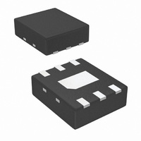
DS38EP100SD/NOPB National Semiconductor, DS38EP100SD/NOPB Datasheet - Page 7

DS38EP100SD/NOPB
Manufacturer Part Number
DS38EP100SD/NOPB
Description
IC EQUALIZER POWER SAVER 6-LLP
Manufacturer
National Semiconductor
Series
PowerWise®r
Datasheet
1.DS38EP100SDNOPB.pdf
(16 pages)
Specifications of DS38EP100SD/NOPB
Applications
*
Interface
*
Voltage - Supply
*
Package / Case
6-LLP
Mounting Type
Surface Mount
For Use With
DS38EP100EVKH - BOARD EVAL FOR DS38EP100 HDMIDS38EP100EVK - BOARD EVAL FOR DS38EP100
Lead Free Status / RoHS Status
Lead free / RoHS Compliant
Other names
DS38EP100SDTR
Application Information
DS38EP100 DEVICE DESCRIPTION
The DS38EP100 Power-Saver equalizer is a passive network
circuit composed of resistive, capacitive, and inductive com-
ponents (See Figure 4). A differential bridged T-network com-
pensates for the transmission medium losses and minimizes
medium-induced deterministic jitter with FR4 and cables. The
equalizer attenuates low frequency signals and is a bandpass
filter at the resonant frequency. The response is linear and
symmetric.
I/O TERMINATIONS
The DS38EP100 I/O impedance is 100Ω differential. The
equalizer is designed for 100Ω-balanced differential signals
and is not intended for single-ended transmission.
LINEAR COMPENSATION
The unique linear compensation feature of the DS38EP100
combined with the tiny package allows maximum flexibility in
placement. The equalizer can be placed anywhere in the data
7
path and will provide the same compensation at the receiving
circuit. (See Simplified Application Diagram)
SYMMETRIC I/O STRUCTURES
The symmetry of the passive equalization network allows bi-
directional operation. Signals receive equal compensation
regardless of the direction of data flow. (See Figure 4).
PCB LAYOUT CONSIDERATIONS FOR DIFFERENTIAL
PAIRS AND NO CONNECT PADS
The differential I/Os must have a controlled differential
impedance of 100Ω. It is preferable to route all differential
lines exclusively on one layer of the board. The use of vias
should be avoided if possible. If vias must be used, they
should be used sparingly and must be placed symmetrically
for each side of a given differential pair. Differential signals
should be routed away from other signals and noise sources
on the printed circuit board. Pin 2, Pin 5, and the center DAP
have to be left as a no connect. Therefore, do not connect the
landing pads of these pins to the power or ground plane. See
AN-1187 for additional information on the LLP package.
www.national.com


