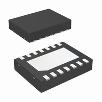
DS64EV100SD/NOPB National Semiconductor, DS64EV100SD/NOPB Datasheet - Page 4

DS64EV100SD/NOPB
Manufacturer Part Number
DS64EV100SD/NOPB
Description
IC EQUALIZER SGL PROGR 14-LLP
Manufacturer
National Semiconductor
Series
PowerWise®r
Datasheet
1.DS64EV100SDNOPB.pdf
(10 pages)
Specifications of DS64EV100SD/NOPB
Applications
Displays
Interface
Coax Cable and Female Connector
Voltage - Supply
2.5V, 3.3V
Package / Case
14-LLP
Mounting Type
Surface Mount
Lead Free Status / RoHS Status
Lead free / RoHS Compliant
Other names
DS64EV100SD
DS64EV100SD
DS64EV100SDTR
DS64EV100SD
DS64EV100SDTR
Available stocks
Company
Part Number
Manufacturer
Quantity
Price
Company:
Part Number:
DS64EV100SD/NOPB
Manufacturer:
National Semiconductor
Quantity:
1 955
Company:
Part Number:
DS64EV100SD/NOPB
Manufacturer:
TI
Quantity:
118
www.national.com
R
R
CML OUTPUTS (OUT+, OUT−)
V
V
t
R
R
t
t
EQUALIZATION
DJ1
DJ2
DJ3
DJ4
RJ
R
PLHD
PHLD
Symbol
OD
OCM
LI
IN
O
LO
, t
Note 1: “Absolute Maximum Ratings” indicate limits beyond which damage to the device may occur, including inoperability and degradation of device reliability
and/or performance. Functional operation of the device and/or non-degradation at the Absolute Maximum Ratings or other conditions beyond those indicated in
the Recommended Operating Conditions is not implied. The Recommended Operating Conditions indicate conditions at which the device is functional and the
device should not be operated beyond such conditions. Absolute Maximum Numbers are guaranteed for a junction temperature range of –40°C to +125°C. Models
are validated to Maximum Operating Voltages only.
Note 2: Typical values represent most likely parametric norms at V
product characterization and are not guaranteed.
Note 3: The Electrical Characteristics tables list guaranteed specifications under the listed Recommended Operating Conditions except as otherwise modified
or specified by the Electrical Characteristics Conditions and/or Notes. Typical specifications are estimations only and are not guaranteed.
Note 4: Allowed supply noise (mV
Note 5: Specification is guaranteed by characterization at optimal boost setting and is not tested in production.
Note 6: Deterministic jitter is measured at the differential outputs (point C of Figure 1), minus the deterministic jitter before the test channel (point A of Figure 1).
Random jitter is removed through the use of averaging or similar means.
Note 7: Measured with clock-like {11111 00000} pattern.
Note 8: Random jitter contributed by the equalizer is defined as sqrt (J
J
Note 9: The V
IN
F
is the random jitter at the input of the equalizer in ps
Differential Input
Return Loss
Input Resistance
Output Differential
Voltage Level (OUT
diff)
Output Common-
Mode Voltage
Transition Time
Output Resistance
Differential Output
Return Loss
Differential Low to
High Propagation
Delay
Differential High to
Low Propagation
Delay
Residual
Deterministic Jitter at
10 Gbps
Residual
Deterministic Jitter at
6.4 Gbps
Residual
Deterministic Jitter at
5 Gbps
Residual
Deterministic Jitter at
2.5 Gbps
Random Jitter
DD2.5
Parameter
is V
DD
= 2.5V ± 5% and V
P-P
sine wave) under typical conditions.
100 MHz – 3.2 GHz, with fixture’s effect de-
embedded
Differential Across IN+ and IN-. (Figure 4)
Differential measurement with OUT+ and OUT-
terminated by 50Ω to GND, AC-Coupled
(Figure 2)
Single-ended measurement DC-Coupled with
50Ω terminations
(Note 7)
20% to 80% of differential output voltage,
measured within 1” from output pins.
(Figure 2)
(Note 7)
Single-ended to V
100 MHz – 1.6 GHz, with fixture’s effect de-
embedded. IN+ = static high.
Propagation delay measurement at 50% V
between input to output, 100 Mbps
(Figure 3), (Note 7)
30” of 6 mil microstrip FR4, EQ Setting 0x06,
PRBS-7 (2
(Note 5, 6)
40” of 6 mil microstrip FR4, EQ Setting 0x06,
PRBS-7 (2
(Note 5, 6)
40” of 6 mil microstrip FR4, EQ Setting 0x07,
PRBS-7 (2
(Note 5, 6)
40” of 6 mil microstrip FR4, EQ Setting 0x07,
PRBS-7 (2
(Note 5, 6)
(Note 7, 8)
DD3.3
is V
7
7
7
7
DD
-1) pattern
-1) pattern
-1) pattern
-1) pattern
rms
= 3.3V ± 10%.
, see Figure 1.
Conditions
DD
DD
= 3.3V or 2.5V, T
OUT
2
– J
IN
4
2
). J
OUT
A
is the random jitter at equalizer outputs in ps
= 25°C., and at the Recommended Operation Conditions at the time of
OD
V
DD
Min
550
85
20
42
-0.2
(Note 2)
0.20
0.17
0.12
0.10
Typ
100
620
240
240
0.5
10
50
10
rms
, see point C of Figure 1;
V
DD
Max
0.26
0.20
0.16
115
725
60
58
-0.1
mV
Units
ps
UI
UI
UI
UI
dB
dB
ps
ps
ps
Ω
Ω
V
P-P
P-P
P-P
P-P
rms
P-P


