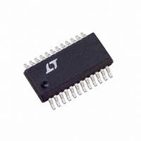
LTC4306CGN#TR Linear Technology, LTC4306CGN#TR Datasheet - Page 4

LTC4306CGN#TR
Manufacturer Part Number
LTC4306CGN#TR
Description
IC MUX 4CH 2-WIRE BUS 24-SSOP
Manufacturer
Linear Technology
Datasheet
1.LTC4306CUFDPBF.pdf
(20 pages)
Specifications of LTC4306CGN#TR
Applications
Multiplexer with Amplifier
Interface
SMBus (2-Wire/I²C)
Voltage - Supply
2.2 V ~ 5.5 V
Package / Case
24-SSOP
Mounting Type
Surface Mount
Lead Free Status / RoHS Status
Contains lead / RoHS non-compliant
Available stocks
Company
Part Number
Manufacturer
Quantity
Price
LTC4306
ELECTRICAL CHARACTERISTICS
range, otherwise specifications are at T
4
Note 1: Absolute Maximum Ratings are those values beyond which the life
of a device may be impaired.
Note 2: Guaranteed by design and not subject to test.
Note 3: The boosted pull-up currents are regulated to prevent excessively
fast edges for light loads. See the Typical Performance Characteristics for
rise time as a function of V
I
Note 4: When a logic low voltage, V
Upstream-Downstream Buffers, the voltage on the other side is regulated
SYMBOL
V
V
I
V
V
I
I
I
V
V
I
C
V
I
f
t
t
t
t
t
t
t
t
t
BOOST
2
ADR(IN, L)
ADR(FLOAT)
ADR(IN, H)
SDAIN,SCLIN(OH)
2
SCL
BUF
HD,STA
SU,STA
SU,STO
HD,DATI
HD,DATO
SU,DAT
f
SP
ALERT1-4(IN)
ALERT1-4(HY)
ADR(H)
ADR(L)
SDAIN,SCLIN(TH)
SDAIN,SCLIN(HY)
IN
SDAIN(OL)
C Interface
C Interface Timing
as a function of V
PARAMETER
ALERT1-ALERT4 Pin Input Falling
Threshold Voltages
ALERT1-ALERT4 Pin Input Threshold
Hysteresis Voltages
ADR0-2 Input High Voltage
ADR0-2 Input Low Voltage
ADR0-2 Logic Low Input Current
ADRO-2 Allowed Input Current
ADR0-2 Logic High Input Current
SDAIN, SCLIN Input Falling Threshold
Voltages
SDAIN, SCLIN Hysteresis
SDAIN, SCLIN Input Current
SDA, SCL Input Capacitance
SDAIN Output Low Voltage
Maximum SCL Clock Frequency
Bus Free Time Between Stop/Start Condition (Note 2)
Hold Time After (Repeated) Start Condition
Repeated Start Condition Set-up Time
Stop Condition Set-up Time
Data Hold Time Input
Data Hold Time Output
Data Set-up Time
SCL, SDA Fall Times
Pulse Width of Spikes Suppressed by the
Input Filter
CC
CC
and temperature.
and parasitic bus capacitance C
LOW
, is forced on one side of the
A
= 25°C. V
CC
BUS
= 3.3V unless otherwise noted.
CONDITIONS
ADR0-2 = 0V, V
V
ADR0-2 = V
V
SCL, SDA = V
(Note 2)
I
(Note 2)
(Note 2)
(Note 2)
(Note 2)
(Note 2)
(Note 2)
(Note 2)
(Note 2)
(Note 2)
and for
SDA
CC
CC
The
= 2.7V, 5.5V (Note 5)
= 5.5V
= 4mA, V
●
denotes specifications which apply over the full specified temperature
CC
CC
CC
= 5.5V
to a voltage V
V
pin (e.g., SDAIN) and V
LTC4306 is driving the downstream pin (e.g., SDA1). See the Typical
Performance Characteristics for V
function of V
Note 5: When floating, the ADR0-ADR2 pins can tolerate pin leakage
currents up to I
CC
OS,UP-BUF
= 2.7V
= 5.5V
is the offset voltage when the LTC4306 is driving the upstream
CC
LOW2
ADR(FLOAT)
and bus pull-up current.
= V
LOW
OS,DOWN-BUF
and still convert the address correctly.
+ V
●
●
●
●
●
●
●
●
●
OS
, where V
OS,UP-BUF
20 + 0.1 •
0.1 • V
is the offset voltage when the
C
MIN
–30
400
300
0.8
1.4
±5
30
50
BUS
CC
OS
and V
0.75 • V
0.25 • V
is a positive offset voltage.
0.75
TYP
–60
±13
–30
–30
–25
600
150
1.0
1.6
0.2
80
60
30
45
50
OS,DOWN-BUF
0
6
CC
CC
0.9 • V
MAX
–80
100
900
100
300
250
1.2
1.8
0.4
1.3
± 5
80
0
0
0
as a
CC
UNITS
4306f
kHz
mV
mV
µA
µA
µA
µA
pF
µs
ns
ns
ns
ns
ns
ns
ns
ns
V
V
V
V
V


