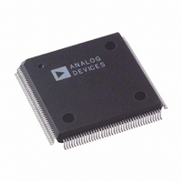
AD9887AKSZ-170 Analog Devices Inc, AD9887AKSZ-170 Datasheet - Page 13

AD9887AKSZ-170
Manufacturer Part Number
AD9887AKSZ-170
Description
IC INTRFACE ANALOG/DVI 160-MQFP
Manufacturer
Analog Devices Inc
Specifications of AD9887AKSZ-170
Applications
Graphic Cards, VGA Interfaces
Interface
Analog and Digital
Voltage - Supply
3.15 V ~ 3.45 V
Package / Case
160-MQFP, 160-PQFP
Mounting Type
Surface Mount
Supply Voltage Range
3.15V To 3.45V, 2.2V To 3.45V
Operating Temperature Range
0°C To +70°C
Digital Ic Case Style
MQFP
No. Of Pins
160
Msl
MSL 3 - 168 Hours
Termination Type
SMD
Rohs Compliant
Yes
Filter Terminals
SMD
Bandwidth
170MHz
Lead Free Status / RoHS Status
Lead free / RoHS Compliant
Available stocks
Company
Part Number
Manufacturer
Quantity
Price
Company:
Part Number:
AD9887AKSZ-170
Manufacturer:
ADI
Quantity:
437
Company:
Part Number:
AD9887AKSZ-170
Manufacturer:
Analog Devices Inc
Quantity:
10 000
Part Number:
AD9887AKSZ-170
Manufacturer:
AD
Quantity:
20 000
PIN FUNCTION DETAILS—ANALOG INTERFACE
Analog Video Data Inputs
R
G
B
External Inputs
HSYNC
VSYNC
Sync/Clock Inputs
SOGIN
AIN
AIN
AIN
Sync-on-Green Input
Analog Input for Red Channel
Analog Input for Green Channel
Analog Input for Blue Channel
These are the high impedance inputs that accept
graphics signals from the red, green, and blue
channels, respectively. For RGB, the three channels
are identical and can be used for any color, but colors
are assigned for convenient reference. For proper
4:2:2 formatting in a YUV application, the Y channel
must be connected to the G
connected to the B
connected to the R
These pins accommodate input signals ranging from
0.5 V to 1.0 V full scale. Signals should be ac-coupled
to these pins to support clamp operation.
Horizontal Sync Input
This input receives a logic signal that establishes the
horizontal timing reference and provides the fre-
quency reference for pixel clock generation.
The logic sense of this pin is controlled by Serial
Register 0x0F, Bit 7 (Hsync polarity). Only the leading
edge of Hsync is active; the trailing edge is ignored.
When Hsync polarity = 0, the falling edge of Hsync
is used. When Hsync polarity = 1, the rising edge is
active.
The input includes a Schmitt trigger for noise
immunity with a nominal input threshold of 1.5 V.
Electrostatic discharge (ESD) protection diodes
conduct heavily if this pin is driven more than 0.5 V
above the maximum tolerance voltage (3.3 V) or
more than 0.5 V below ground.
Vertical Sync Input
This is the input for vertical sync.
This input is provided to assist with processing
signals with embedded sync, typically on the green
channel. The pin is connected to a high speed com-
parator with an internally generated threshold that is
0.15 V above the negative peak of the input signal.
When connected to an ac-coupled graphics signal
with embedded sync, it produces a noninverting
digital output on SOGOUT.
AIN
AIN
input, and V must be
input.
AIN
input, U must be
Rev. B | Page 13 of 52
CLAMP
COAST
CKEXT
When not used, leave this input unconnected. For
more details on this function and how it should be
configured, refer to the Sync-on-Green Input section.
External Clamp Input (Optional)
This logic input can be used to define the time
during which the input signal is clamped to the
reference dc level (ground for RGB, midscale for
YUV). It should be used when the reference dc level
is known to be present on the analog input channels,
typically during a period called the back porch of
the graphics signal following Hsync. The CLAMP
pin is enabled by setting control bit EXTCLMP to 1
(the default at power-up is 0). When disabled, this
pin is ignored and the clamp timing is determined
internally by counting the delay and duration from
the trailing edge of the HSYNC input. The logic
sense of this pin is controlled by CLAMPOL. When
not used, this pin must be grounded and EXTCLMP
must be programmed to 0.
Clock Generator Coast Input (Optional)
This input can be used to stop the pixel clock generator
from synchronizing with Hsync while maintaining
the clock at its current frequency and phase. This is
useful when processing signals from sources that
fail to produce horizontal sync pulses when in the
vertical interval. The coast signal is generally not
required for PC-generated signals. For applications
requiring coast, it is provided through the internal
coast found in the sync processing engine.
The logic sense of this pin is controlled by coast
polarity. When not used, this pin can be grounded
with coast polarity programmed to 1, or tied high
with coast polarity programmed to 0. Coast polarity
defaults to 1 at power-up.
External Clock Input (Optional)
This pin can be used to provide an external clock to
the AD9887A in place of the clock internally
generated from HSYNC. It is enabled by program-
ming CKEXT to 1. When an external clock is used,
all other internal functions, including the clock
phase adjustment, operate normally. When not
used, this pin should be tied to V
and CKEXT should be programmed to 0.
DD
or to ground
AD9887A


