NIS1050MNTBG ON Semiconductor, NIS1050MNTBG Datasheet - Page 2
NIS1050MNTBG
Manufacturer Part Number
NIS1050MNTBG
Description
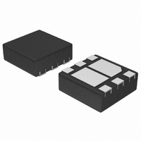
IC PMIC INTERFACE PROTECT 6-WDFN
Manufacturer
ON Semiconductor
Datasheet
1.NIS1050MNTBG.pdf
(5 pages)
Specifications of NIS1050MNTBG
Applications
Mobile Communications
Voltage - Supply
3 V ~ 30 V
Package / Case
6-VDFN Exposed Pad
Mounting Type
Surface Mount
Lead Free Status / RoHS Status
Lead free / RoHS Compliant
Interface
-
Lead Free Status / Rohs Status
Lead free / RoHS Compliant
Available stocks
Company
Part Number
Manufacturer
Quantity
Price
Company:

Part Number:
NIS1050MNTBG
Manufacturer:
ON
Quantity:
3 609
Company:
Part Number:
NIS1050MNTBG
Manufacturer:
ON Semiconductor
Quantity:
800
Part Number:
NIS1050MNTBG
Manufacturer:
ON/安森美
Quantity:
20 000


Stresses exceeding Maximum Ratings may damage the device. Maximum Ratings are stress ratings only. Functional operation above the
Recommended Operating Conditions is not implied. Extended exposure to stresses above the Recommended Operating Conditions may affect
device reliability.
1. Surface Mounted on FR4 Board using the minimum recommended pad size of 30 mm
2. Dual die operation (equally−heated).
3. Surface Mounted on FR4 Board using 1 in sq pad size (Cu area = 1.127 in sq [2 oz] including traces).
4. Surface Mounted on FR4 Board using the minimum recommended pad size (30 mm
SINGLE DIE OPERATION (SELF-HEATED)
DUAL DIE OPERATION (EQUALLY-HEATED)
Table 1. FUNCTIONAL PIN DESCRIPTION
Table 2. MAXIMUM RATINGS
Table 3. THERMAL RESISTANCE RATINGS
Input Voltage, Operating, Steady-State (OVP_sense to Gnd)
Gate-to-Source Voltage
Drain Current, Peak (10 ms pulse)
Drain Current, Continuous (Note 1, Steady-State)
T
T
Total Power Dissipation @ T
Operating Temperature Range
Non-operating Temperature Range
Maximum Lead Temperature for Soldering Purposes
Junction-to-Ambient – Steady State (Note 3)
Junction-to-Ambient – Steady State Min Pad (Note 4)
Junction-to-Ambient – t ≤ 5 s (Note 3)
Junction-to-Ambient – Steady State (Note 3)
Junction-to-Ambient – Steady State Min Pad (Note 4)
Junction-to-Ambient – t ≤ 5 s (Note 3)
A
A
= 25°C
= 85°C
3, 7
6, 8
Pin
1
2
4
5
Function
Ground
Source
Drain
Gate
Vout
Vin
A
= 25°C (Note 1, 2)
This is the source of the power FET and connects to the PMIC pin of the same name.
This pin is the gate of the FET switch.
Positive input voltage to the device.
Negative input voltage to the device. This is used as the internal reference for the IC.
This is the output of the internal LDO. It passes the input voltage through to the output and clamps
that voltage if it exceeds the regulation limit.
Positive input voltage to the device.
Parameter
Rating
Figure 3. Pin Assignment
http://onsemi.com
1
2
3
8
7
2
6
5
4
Description
2
, 2 oz Cu).
2
, 2 oz Cu.
Symbol
Symbol
P
R
R
R
R
R
R
V
I
V
Dpk
T
T
T
I
max
qJA
qJA
qJA
qJA
qJA
qJA
GS
D
in
J
J
L
-40 to 125
-55 to 150
-0.3 to 30
Value
Max
750
260
177
133
3.7
2.7
±8
20
83
54
58
40
°C/W
°C/W
Unit
Unit
mW
°C
°C
°C
V
V
A
A
Related parts for NIS1050MNTBG
Image
Part Number
Description
Manufacturer
Datasheet
Request
R

Part Number:
Description:
Protection Interface Circuit For Pmics With Integrated Ovp Control
Manufacturer:
ON Semiconductor
Datasheet:
Part Number:
Description:
ON Semiconductor [VOLTAGE REGULATOR]
Manufacturer:
ON Semiconductor
Datasheet:
Part Number:
Description:
357-036-542-201 CARDEDGE 36POS DL .156 BLK LOPRO
Manufacturer:
ON Semiconductor
Datasheet:
Part Number:
Description:
357-036-542-201 CARDEDGE 36POS DL .156 BLK LOPRO
Manufacturer:
ON Semiconductor
Datasheet:
Part Number:
Description:
357-036-542-201 CARDEDGE 36POS DL .156 BLK LOPRO
Manufacturer:
ON Semiconductor
Datasheet:
Part Number:
Description:
357-036-542-201 CARDEDGE 36POS DL .156 BLK LOPRO
Manufacturer:
ON Semiconductor
Datasheet:
Part Number:
Description:
357-036-542-201 CARDEDGE 36POS DL .156 BLK LOPRO
Manufacturer:
ON Semiconductor
Datasheet:
Part Number:
Description:
357-036-542-201 CARDEDGE 36POS DL .156 BLK LOPRO
Manufacturer:
ON Semiconductor
Datasheet:
Part Number:
Description:
357-036-542-201 CARDEDGE 36POS DL .156 BLK LOPRO
Manufacturer:
ON Semiconductor
Datasheet:
Part Number:
Description:
357-036-542-201 CARDEDGE 36POS DL .156 BLK LOPRO
Manufacturer:
ON Semiconductor
Datasheet:
Part Number:
Description:
357-036-542-201 CARDEDGE 36POS DL .156 BLK LOPRO
Manufacturer:
ON Semiconductor
Datasheet:
Part Number:
Description:
357-036-542-201 CARDEDGE 36POS DL .156 BLK LOPRO
Manufacturer:
ON Semiconductor
Datasheet:
Part Number:
Description:
Manufacturer:
ON Semiconductor
Datasheet:
Part Number:
Description:
Manufacturer:
ON Semiconductor
Datasheet: