MAX1558ETB+T Maxim Integrated Products, MAX1558ETB+T Datasheet - Page 2
MAX1558ETB+T
Manufacturer Part Number
MAX1558ETB+T
Description
IC CURR-LIM SW DUAL PROG 10-TDFN
Manufacturer
Maxim Integrated Products
Datasheet
1.MAX1558ETBT.pdf
(14 pages)
Specifications of MAX1558ETB+T
Applications
USB
Interface
USB
Voltage - Supply
2.75 V ~ 5.5 V
Package / Case
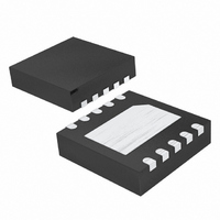
10-TDFN Exposed Pad
Mounting Type
Surface Mount
Lead Free Status / RoHS Status
Lead free / RoHS Compliant


ABSOLUTE MAXIMUM RATINGS
IN_, ON_, OUT_, ISET, FLT_ to GND........................-0.3V to +6V
IN_ to OUT_ (when disabled) (Note 1) ........................-6V to +6V
IN_ to OUT_ (when enabled) (Note 2)............-1.6A to +1.6A
FLT_ Sink Current................................................................20mA
Dual, 3mm x 3mm, 1.2A/Programmable-Current
USB Switches with Autoreset
Stresses beyond those listed under “Absolute Maximum Ratings” may cause permanent damage to the device. These are stress ratings only, and functional
operation of the device at these or any other conditions beyond those indicated in the operational sections of the specifications is not implied. Exposure to
absolute maximum rating conditions for extended periods may affect device reliability.
ELECTRICAL CHARACTERISTICS
(V
unless otherwise noted. Typical values are at T
2
Note 1: Reverse current (current from OUT_ to IN_) is blocked when disabled.
Note 2: Forward current (current from IN_ to OUT_) is internally limited. Reverse current, from OUT_ to IN_, is not limited when the
Supply Voltage Range
Switch On-Resistance
Standby Supply Current
Quiescent Supply Current
OUT_ Off-Leakage Current
Reverse Leakage Current
Undervoltage-Lockout Threshold
Continuous Load Current
Current-Limit Threshold
Peak Short-Circuit Current Limit
RMS Short-Circuit Current Limit
Short-Circuit Continuous Current-
Limit Transition Threshold
Fault-Blanking Timeout Period
Turn-On Delay
INA
_______________________________________________________________________________________
= V
device is enabled and must be kept below 1.5A
are disabled, the switch turns off and reverse current is internally blocked.
INB
PARAMETER
= 5V, V
ONA
= V
ONB
= 0V (MAX1558), V
SYMBOL
I
I
V
SHORT
SHORT
R
UVLO
t
ON
ON
A
= +25°C.) (Note 3)
V
V
V
Both switches disabled
Both switches enabled
Switches disabled
V
switches disabled
Rising edge, 3% hysteresis
R
V
0.5V
V
(I
V
(I
(Note 4)
From I
R
include rise time (from ON asserted to
V
IN_
IN_
IN_
IN_
IN_
OUT_
OUT_
OUT_
OUT_
OUT_
ISET
OUT_
ONA
= 5V, T
= 3.3V, T
= 4.4V, T
= 0V, V
- V
= 26kΩ
RMS
LIMIT
= 0V
pulsing)
= 0V
pulsing)
= 10% V
= 10Ω, C
OUT_
= V
RMS
to prevent permanent device damage. When the MAX1558/MAX1558H
ONB
condition to 50% of V
A
OUTA
=
A
A
= +25°C
CONDITIONS
IN_
= +25°C
= 0°C to +85°C
OUT_
= 5V (MAX1558H), R
= V
)
Continuous Power Dissipation (T
Operating Temperature Range ...........................-40°C to +85°C
Junction Temperature ......................................................+160°C
Storage Temperature Range .............................-65°C to +150°C
Lead Temperature (soldering, 10s) .................................+300°C
V
V
R
R
R
R
R
R
R
R
R
OUTB
= 1µF, does not
10-Pin TDFN 3mm x 3mm
(derate 24.4mW/°C above +70°C) .............................1952mW
OUTA
OUTA
ISET
ISET
ISET
ISET
ISET
ISET
ISET
ISET
ISET
= 26kΩ
= 39kΩ
= 60kΩ
= 26kΩ
= 39kΩ
= 60kΩ
= 26kΩ
= 39kΩ
= 60kΩ
= 5V, both
= V
= V
OUTB
OUTB
FLT_
ISET
= 0V
= 5V
= 26kΩ to GND, T
2.75
1.20
0.80
0.50
1.45
MIN
2.3
1.2
0.5
8
A
= +70°C)
0.925
TYP
0.03
0.03
0.03
1.40
0.90
0.55
0.37
0.23
2.5
1.4
0.6
2.0
1.4
55
64
45
20
3
1
A
= 0°C to +85°C,
MAX
5.50
1.60
1.05
0.70
2.60
105
2.7
4.0
75
75
10
40
6
A
UNITS
A
(PEAK)
mΩ
µA
µA
µA
µA
RMS
ms
ms
V
V
A
A
V
Related parts for MAX1558ETB+T
Image
Part Number
Description
Manufacturer
Datasheet
Request
R

Part Number:
Description:
MAX CLIP
Manufacturer:
Aavid Thermalloy
Datasheet:

Part Number:
Description:
MAX7528KCWPMaxim Integrated Products [CMOS Dual 8-Bit Buffered Multiplying DACs]
Manufacturer:
Maxim Integrated Products
Datasheet:
Part Number:
Description:
Single +5V, fully integrated, 1.25Gbps laser diode driver.
Manufacturer:
Maxim Integrated Products
Datasheet:
Part Number:
Description:
Single +5V, fully integrated, 155Mbps laser diode driver.
Manufacturer:
Maxim Integrated Products
Datasheet:
Part Number:
Description:
VRD11/VRD10, K8 Rev F 2/3/4-Phase PWM Controllers with Integrated Dual MOSFET Drivers
Manufacturer:
Maxim Integrated Products
Datasheet:
Part Number:
Description:
Highly Integrated Level 2 SMBus Battery Chargers
Manufacturer:
Maxim Integrated Products
Datasheet:
Part Number:
Description:
Current Monitor and Accumulator with Integrated Sense Resistor; ; Temperature Range: -40°C to +85°C
Manufacturer:
Maxim Integrated Products
Part Number:
Description:
TSSOP 14/A�/RS-485 Transceivers with Integrated 100O/120O Termination Resis
Manufacturer:
Maxim Integrated Products
Part Number:
Description:
TSSOP 14/A�/RS-485 Transceivers with Integrated 100O/120O Termination Resis
Manufacturer:
Maxim Integrated Products
Part Number:
Description:
QFN 16/A�/AC-DC and DC-DC Peak-Current-Mode Converters with Integrated Step
Manufacturer:
Maxim Integrated Products
Part Number:
Description:
TDFN/A/65V, 1A, 600KHZ, SYNCHRONOUS STEP-DOWN REGULATOR WITH INTEGRATED SWI
Manufacturer:
Maxim Integrated Products
Part Number:
Description:
Integrated Temperature Controller f
Manufacturer:
Maxim Integrated Products
Part Number:
Description:
SOT23-6/I�/45MHz to 650MHz, Integrated IF VCOs with Differential Output
Manufacturer:
Maxim Integrated Products
Part Number:
Description:
SOT23-6/I�/45MHz to 650MHz, Integrated IF VCOs with Differential Output
Manufacturer:
Maxim Integrated Products
Part Number:
Description:
EVALUATION KIT/2.4GHZ TO 2.5GHZ 802.11G/B RF TRANSCEIVER WITH INTEGRATED PA
Manufacturer:
Maxim Integrated Products