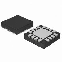
NCN4557MTR2G ON Semiconductor, NCN4557MTR2G Datasheet

NCN4557MTR2G
Specifications of NCN4557MTR2G
Available stocks
Related parts for NCN4557MTR2G
NCN4557MTR2G Summary of contents
Page 1
... POS Terminals (SAM Card Interfaces) • Smart Card Readers *For additional information on our Pb−Free strategy and soldering details, please download the ON Semiconductor Soldering and Mounting Techniques Reference Manual, SOLDERRM/D. © Semiconductor Components Industries, LLC, 2006 June, 2006 − Rev. 0 http://onsemi.com ...
Page 2
NCN4557 BAT 1 5 5.5 V 0 CRD_V BAT ENABLE CRD_RSTA 12 P4 SEL0 CRD_CLKA 11 SEL1 P3 CRD_I/OA 9 ...
Page 3
LDO B > CRD_V B CC 1.8 V/3.0 V/Enable CRD_V CRD_CLKB En 15 CRD_RSTB En I/O DATA 14 CRD_I/OB I CRD_V CLK RST 9 I ...
Page 4
PIN DESCRIPTIONS PIN Name Type 1 CRD_V B POWER This pin is connected to the Card power supply pin (C1) (Card B).The corresponding LDO is CC programmable using the pins SEL0, SEL1 and ENABLE to provide 1.8 V, 3.0 V ...
Page 5
ATTRIBUTES ESD protection Human Body Model (HBM): Card Pins ( 14 & 17) (Note 1) Machine Model (MM): Charged Device Model (CDM): Moisture sensitivity (Note 2) Flammability Rating Meets or exceeds JEDEC Spec ...
Page 6
POWER SUPPLY SECTION (−40°C to +85°C) Pin Symbol 3 V Power Supply BAT 3 I Operating current VBAT CRD_V A = 3.0 V, CRD_V CC CRD_V A = 1.8 V, CRD_V CC CRD_V CRD_V CC CRD_V ...
Page 7
CARD INTERFACE SECTION (−40°C to +85°C) Pin Symbol 6,15 CRD_RSTA CRD_V = + CRD_RSTB Output RESET V Output RESET V Output RESET Rise Time @ C Output RESET Fall Time @ C CRD_V = +1 Output ...
Page 8
Drop−out 26 CRD_V A CRD_V A 2.7 3.1 3.5 3.9 4.3 V (V) BAT Figure 4. I Operating Current vs. V BAT T = 25° ...
Page 9
The NCN4557 is a dual LDO−based DC/DC converter and level shifter able to handle independently 2 smart card interfaces. When one of these interfaces is operating the other one is not active and conversely. Class B (3.0 V) and C ...
Page 10
I/O IO/CONTROL The typical waveform provided in Figure 11 shows how the accelerator operates. During the first 200 ns (typical), the slope of the rise time is solely a function of the pullup resistor associated with ...
Page 11
... V Figure 14. Typical Schmitt Trigger Characteristics ORDERING INFORMATION Device NCN4557MTG NCN4557MTR2G †For information on tape and reel specifications, including part orientation and tape sizes, please refer to our Tape and Reel Packaging Specifications Brochure, BRD8011/D. NCN4557 Shutdown Operating In order to save power or for other purpose required by the application it is possible to put the NCN4557 in a shutdown mode by setting LOW the pin ENABLE ...
Page 12
... SCILLC is an Equal Opportunity/Affirmative Action Employer. This literature is subject to all applicable copyright laws and is not for resale in any manner. PUBLICATION ORDERING INFORMATION LITERATURE FULFILLMENT: Literature Distribution Center for ON Semiconductor P.O. Box 5163, Denver, Colorado 80217 USA Phone: 303−675−2175 or 800−344−3860 Toll Free USA/Canada Fax: 303− ...


