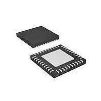
MAX14502AETL+ Maxim Integrated Products, MAX14502AETL+ Datasheet - Page 23

MAX14502AETL+
Manufacturer Part Number
MAX14502AETL+
Description
IC CARD READER USB-SD 40-TQFN
Manufacturer
Maxim Integrated Products
Type
Smart Card Interface ICr
Datasheet
1.MAX14502AETL.pdf
(41 pages)
Specifications of MAX14502AETL+
Applications
USB
Interface
I²C
Voltage - Supply
1.8 V ~ 3.3 V
Package / Case
40-TQFN Exposed Pad
Mounting Type
Surface Mount
Maximum Operating Temperature
+ 85 C
Minimum Operating Temperature
- 40 C
Mounting Style
SMD/SMT
Lead Free Status / RoHS Status
Lead free / RoHS Compliant
The control register controls the settings of SD port
analog switches, Card Reader mode, and sleep (Table
2.) The state of the SD port analog switches can be
changed when the device is in Sleep mode or in Card
Reader mode, and actions are executed immediately. If
SD card 1 is connected to the PC through USB in Card
Reader mode, the state of the SD port 1 switches are
ignored, but the SD port 2 switches can still be con-
trolled through the Control register. Likewise, if SD card
2 is connected to the USB connector in Card Reader
mode, the state of the SD port 2 switches are ignored,
but the SD port 1 switches can still be controlled
through the Control register. Changing the card reader
bits in Sleep mode does not cause the device to enter
Card Reader mode. Under this condition, the
MAX14500–MAX14503 enter Card Reader mode upon
waking up.
Figure 10. I2C_SEL Connected Low to Enable Simple Control and MODE = 0 to Enable Pass Thru
CONNECTOR
SLOT 1
USB
SD
D+
D-
______________________________________________________________________________________
4
CCRD_PRST
CCLK1
CCMD1
CDAT1_[3:0]
CD+
CD-
Control Register (0x00)
TRANSCEIVER
SD CARD INTERFACE
USB
CARD READER
USB HS
USB SWITCHES
Hi-Speed USB-to-SD Card
MAX14500–
MAX14503
SD PORT 1 SWITCHES
The MAX14500–MAX14503 have three configuration reg-
isters (CONFIG1 = 0x01, CONFIG2 = 0x02, CONFIG3 =
0x03). The configuration registers control the SD bus
bit data mode, interrupt polarity, interrupt clearance,
clock configuration, SD clock, and USB speed for Card
Reader mode. The default settings are shown in the
Register Map section.
All interrupts are masked in the default reset state.
There are two interrupt enable registers (IE1 = 0x04, IE2
= 0x05) and two interrupt request registers (IRQ1 =
0x10, IRQ2 = 0x11). The BERR/INT output functions as
the bridge error output BERR in simple control and func-
tions as an interrupt INT in I
INT and how INT is asserted can be programmed in
CONFIG1. The INT output asserts for enabled interrupts
and errors in Card Reader mode. The polarity of INT can
be active-high or active-low, and INT can be pro-
Readers with Bypass
HDAT1_[3:0]
HCRD_PRST
I2C_SEL = LOW
MODE = LOW
HCMD1
HCLK1
BUSY
BERR
HD+
HD-
Configuration Registers
4
2
PORT1
HOST
C control. The polarity of
USB
SD
HOST PROCESSOR
I/O
Interrupts (INT)
23


