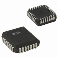
SY100E446JC Micrel Inc, SY100E446JC Datasheet - Page 7

SY100E446JC
Manufacturer Part Number
SY100E446JC
Description
IC CONV 4-BIT SER/PAR 28-PLCC
Manufacturer
Micrel Inc
Datasheet
1.SY100E446JZ_TR.pdf
(9 pages)
Specifications of SY100E446JC
Applications
*
Interface
*
Voltage - Supply
*
Package / Case
28-LCC (J-Lead)
Mounting Type
Surface Mount
Lead Free Status / RoHS Status
Contains lead / RoHS non-compliant
Available stocks
Company
Part Number
Manufacturer
Quantity
Price
Company:
Part Number:
SY100E446JC
Manufacturer:
MICREL
Quantity:
6 219
Micrel, Inc.
converters. The chips are designed to work with the E445
device to provide both transmission and receiving of a high-
speed serial data path. The E446 can convert 4 bits of
data into a 1.3Gb/s NRZ data stream. The device features
a SYNC input which allows the user to reset the internal
clock circuitry and restart the conversion sequence (see
Timing Diagram A). Note that SOUT is triggered by negative
clock edges.
divide-by-eight circuitry to facilitate the cascading of two
devices to build an 8:1 multiplexer. Figure 1 illustrates the
architecture for an 8:1 multiplexer using two E446s (see
Timing Diagram B). Notice the serial outputs (SOUT) of the
lower order converter feed the serial inputs of the higher
order device. This feed through of the serial inputs bounds
the upper end of the frequency of operation. The clock-to-
serial output propagation delay, plus the set-up time of the
M9999-032206
hbwhelp@micrel.com or (408) 955-1690
APPLICATIONS INFORMATION
The SY10E/100E446 are integrated 4:1 parallel-to-serial
The E446 features a differential serial input and internal
t
CLK to SOUT
PD
CLK
CLK
CLK
Figure 1. Cascaded 8:1 Converter Architecture
D
D
3
7
D
D
2
6
D
D
E446B
SOUT
SOUT
1
5
PARALLEL DATA
D
D
0
4
7
1400ps
serial input pins, must fit into a single clock period for the
cascade architecture to function properly. Using the worst
case values for these two parameters from the data sheet,
t
a minimum period of 1400ps or a clock frequency of
700MHz.
single converter. In order to increase this frequency, it is
recommended that the clock edge feeding the E446A be
delayed with respect to the E446B, as shown in Figure 2.
to the first is to take advantage of the differential clock
inputs of the E446. By connecting the clock for E446A to
the complimentary clock input pin, the device will clock a
half a clock period after E446B (Figure 2). Utilizing this
simple technique will raise the potential conversion frequency
up to the maximum 1.3GHz of a stand-alone E446.
PD
1600ps
The clock frequency is somewhat lower than that of a
Perhaps the easiest way to delay the second clock relative
CLK to SOUT = 1600ps and t
SIN
SIN
D
D
3
3
D
D
2
2
D
D
E446A
SOUT
SOUT
1
1
D
D
200ps
0
0
SERIAL
DATA
s
for SIN = –200ps, yields
SY100E446
SY10E446


