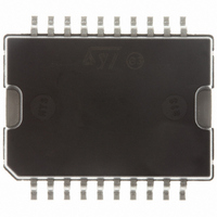
LNBS21PD STMicroelectronics, LNBS21PD Datasheet - Page 16

LNBS21PD
Manufacturer Part Number
LNBS21PD
Description
IC LNB SUPPLY & CNTRL 20-PWRSOIC
Manufacturer
STMicroelectronics
Datasheet
1.LNBS21PD-TR.pdf
(21 pages)
Specifications of LNBS21PD
Applications
Power Supplies, Converters, Controllers
Interface
SMBus (2-Wire/I²C)
Voltage - Supply
8 V ~ 15 V
Package / Case
PowerSO-20 Exposed Bottom Pad
Mounting Type
Surface Mount
Output Voltage
18.7 V
Mounting Style
SMD/SMT
Lead Free Status / RoHS Status
Lead free / RoHS Compliant
Available stocks
Company
Part Number
Manufacturer
Quantity
Price
Company:
Part Number:
LNBS21PD-TR
Manufacturer:
STM
Quantity:
690
LNBS21
Figure 38: Output Voltage Transient Response
from 13V to 18V
V
TERMAL DESIGN NOTES
During normal operation, this device dissipates
some power. At maximum rated output current
(500mA), the voltage drop on the linear regulator
lead to a total dissipated power that is of about
1.7W. The heat generated requires a suitable
heatsink to keep the junction temperature below
the
Assuming
Set-Top-Box case, the total Rthj-amb has to be
less than 50°C/W.
While this can be easily achieved using a
through-hole power package that can be attached
to a small heatsink or to the metallic frame of the
receiver, a surface mount power package must
rely on PCB solutions whose thermal efficiency is
often limited. The simplest solution is to use a
large, continuous copper area of the GND layer to
dissipate the heat coming from the IC body.
The SO-20 package of this IC has 4 GND pins that
are
connection, but also to provide a low thermal
resistance path between the silicon chip and the
PCB heatsink. Given an Rthj-c equal to 15°C/W, a
maximum of 35°C/W are left to the PCB heatsink.
This figure is achieved if a minimum of 25cm
copper area is placed just below the IC body. This
16/21
CC
=12V, I
not
overtemperature
O
=50mA, VSEL=from 0 to 1, EN=1
just
a
40°C
intended
temperature
protection
for
electrical
inside
threshold.
GND
the
2
Figure 39: Output Voltage Transient Response
from 13V to 18V
V
area can be the inner GND layer of a multi-layer
PCB, or, in a dual layer PCB, an unbroken GND
area even on the opposite side where the IC is
placed. In both cases, the thermal path between
the IC GND pins and the dissipating copper area
must exhibit a low thermal resistance.
In figure 40, it is shown a suggested layout for the
SO-20 package with a dual layer PCB, where the
IC Ground pins and the square dissipating area
are thermally connected through 32 vias holes,
filled by solder. This arrangement, when L=50mm,
achieves an Rthc-a of about 25°C/W.
Different
principles, however, suggest to keep the IC and its
ground pins approximately in the middle of the
dissipating area; to provide as many vias as
possible; to design a dissipating area having a
shape as square as possible and not interrupted
by other copper traces.
Due to presence of an exposed pad connected to
GND below the IC body, the PowerSO-20
package has a Rthj-c much lower than the SO-20,
only 2°C/W. As a result, much lower copper area
must be provided to dissipate the same power and
minimum of 12cm
figure 41.
CC
=12V, I
O
=50mA, VSEL=from 1 to 0, EN=1
layouts
2
are
copper area is enough, see
possible,
too.
Basic


