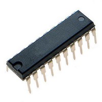
L9705 STMicroelectronics, L9705 Datasheet - Page 3

L9705
Manufacturer Part Number
L9705
Description
IC INTERFACE DOUBLE QUAD 20-DIP
Manufacturer
STMicroelectronics
Datasheet
1.L9705.pdf
(8 pages)
Specifications of L9705
Applications
Monitoring, Digital Current
Voltage - Supply
5 V ~ 25 V
Package / Case
20-DIP (0.300", 7.62mm)
Mounting Type
Through Hole
Mounting Style
Through Hole
Lead Free Status / RoHS Status
Lead free / RoHS Compliant
Interface
-
Lead Free Status / Rohs Status
Lead free / RoHS Compliant
Available stocks
Company
Part Number
Manufacturer
Quantity
Price
Part Number:
L9705D
Manufacturer:
ST
Quantity:
20 000
Company:
Part Number:
L9705D013TR
Manufacturer:
OSRAM
Quantity:
5 149
ELECTRICAL CHARACTERISTCS
(V
specified.)
Notes: 1. The input resistor threshold value is a resistor value from the IN-pin to ground at which the corresponding output changes its status
Symbol
I
V
R
R
V
V
V
S
OUT TS
R
R
V
V
V
I
I
I
t
OUTH
R
t
V
I
I
I
IN
I
I
I
OUT
OUTL
OUT
IN 1,4
IN 5,8
IH 1,4
IH 5,8
R
IL 1,4
IL 5,8
t
dTS
ENH
dIO
ENL
ENh
EN
QC
QS
QS
QC
QS
= 5 to 25V, V
do
IN
IH
IL
(2)
2.
3. The delay times are defined from the crossing point of 50% initiating signal amplitude to the crossing point of 50% output signal
(fig.4)
amplitude
I
IN
Enable Input Voltage LOW
(device activated)
Enable Input Voltage HIGH
Enable Input Threshold
Hysteresis
Enable Input Current
Output Voltage HIGH
Output Current
Output Voltage LOW
Output Current
Output Tristate Current
Input Voltage (device active)
Input Voltage (device active)
Input VoltageDuring Clamp
(device disabled)
Input Resistor LOW Threshold
(note 1)
Input Resistor LOW Threshold
(note 1)
Input Resistor HIGH Threshold
(note 1)
Input Resistor HIGH Threshold
(note 1)
Input Resistor Threshold Ratio
(note 1)
Input Resistor Threshold Ratio
(note 1)
Quiescent Current
Quiescent Current
Quiescent Current
Quiescent Current
Quiescent Current
Quiescent Current
Delay Time/Output (EN LOW to
Output Data Ready) (note 3)
Delay Time/Tristate (EN HIGH to
Output Tristate) (note 3)
Delay Time Input-Output (note 3)
is the sum of the IN5 to IN8 input currents.
CC
Parameter
= 4.75 to 5.25V, V
bat
0V < V
I
EN = HIGH;
5V < V
5V < V
5V < V
5V < V
5V < V
5V < V
V
C
C
2.4V < V
0 < I
OUT status = HIGH; V
OUT status = LOW; V
0 < V
EN = LOW; R
EN = LOW; R
EN = HIGH (t
all contact open
all contact closed
EN = LOW
EN = LOW
EN = LOW; C
OUT
S
OUT
OUT
-0.5V < V
V
V
V
V
V
V
V
= 5 to 16V; T
BAT
BAT
BAT
BAT
BAT
BAT
BAT
OUT
= -1mA
OUT
EN
S
S
S
S
S
S
50pF
50pF
<16V;
<16V;
<16V;
<16V;
<16V;
<16V;
EN
< 100 A
Test Condition
< V
< 0.8V
0.1V
0.1V
0.1V
0.1V
0.1V
0.1V
0.1V
< V
S
CC
ENH
IN
IN
OUT
,< V
CC
BAT
BAT
BAT
BAT
BAT
BAT
BAT
= 1K
= 1K
j
I
I
>20 s)
V
V
V
V
V
V
= -40 to 85°C
IN
IN
GND
GND
GND
GND
GND
GND
50pF
bat
= 30mA
= -30mA
OUT
OUT
-1V , T
= 5.5V
0.1V
0.1V
0.1V
0.1V
0.1V
0.1V
= 0
S
S
S
S
S
S
j
= –40 to 150°C unless otherwise
V
V
Min.
0.05
0.65
0.65
S
-0.3
200
2.4
0.4
1.8
1.8
S
-5
-2
4
+0.3
- 2
V
V
Typ.
0.75
0.75
V
420
0.1
0.5
0.2
1.5
1.5
4.8
5.3
6.5
S
CC
20
-1
-5
-1
4
S
+1
-
-
3R
V
Max.
0.85
0.85
V
V
800
V
-0.3
15+
0.8
0.4
-20
0.5
0.4
S
20
29
40
25
10
35
IN
10
5
2
2
5
8
6
CC
CC
S
·CIN
+2
-
L9705
Unit
mV
mA
mA
mA
mA
K
K
K
K
ms
V
V
V
V
V
V
V
V
A
A
A
A
A
A
A
s
s
3/8


