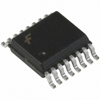
FSAL200QSCX Fairchild Semiconductor, FSAL200QSCX Datasheet - Page 3

FSAL200QSCX
Manufacturer Part Number
FSAL200QSCX
Description
IC MUX/DEMUX QUAD 2X1 16QSOP
Manufacturer
Fairchild Semiconductor
Type
Analog Multiplexerr
Datasheet
1.FSAL200QSCX.pdf
(11 pages)
Specifications of FSAL200QSCX
Function
Multiplexer/Demultiplexer
Circuit
4 x 2:1
On-state Resistance
22 Ohm
Voltage Supply Source
Single Supply
Voltage - Supply, Single/dual (±)
3 V ~ 5.5 V
Current - Supply
1µA
Operating Temperature
-40°C ~ 85°C
Mounting Type
Surface Mount
Package / Case
16-QSOP
On Resistance (max)
22 Ohms
On Time (max)
40 ns
Off Time (max)
20 ns
Supply Voltage (max)
5.5 V
Supply Voltage (min)
3 V
Maximum Power Dissipation
500 mW
Maximum Operating Temperature
+ 85 C
Minimum Operating Temperature
- 40 C
Mounting Style
SMD/SMT
Number Of Switches
Quad
Multiplexer Configuration
Quad 2:1
Number Of Inputs
8
Number Of Outputs
4
Number Of Channels
4
Analog Switch On Resistance
22@3.6V@-40C to 85COhm
Analog Switch Turn On Time
28ns
Analog Switch Turn Off Time
5ns
Package Type
QSOP
Power Supply Requirement
Single
Single Supply Voltage (min)
3V
Single Supply Voltage (typ)
5V
Single Supply Voltage (max)
5.5V
Dual Supply Voltage (min)
Not RequiredV
Dual Supply Voltage (typ)
Not RequiredV
Dual Supply Voltage (max)
Not RequiredV
Power Dissipation
500mW
Mounting
Surface Mount
Pin Count
16
Operating Temp Range
-40C to 85C
Operating Temperature Classification
Industrial
Package
16QSOP
Maximum Data Rate
51.8 Mbps
Maximum On Resistance
22@3.6V Ohm
Maximum High Level Output Current
120 mA
Multiplexer Architecture
2:1
Maximum Turn-off Time
5(Typ)@5.5V ns
Maximum Turn-on Time
28(Typ)@3.6V ns
Power Supply Type
Single
Lead Free Status / RoHS Status
Lead free / RoHS Compliant
Other names
FSAL200QSCX
FSAL200QSCXTR
FSAL200QSCXTR
Available stocks
Company
Part Number
Manufacturer
Quantity
Price
© 2002 Fairchild Semiconductor Corporation
FSAL200 Rev. 1.7.1
Absolute Maximum Ratings
Stresses exceeding the absolute maximum ratings may damage the device. The device may not function or be
operable above the recommended operating conditions and stressing the parts to these levels is not recommended.
In addition, extended exposure to stresses above the recommended operating conditions may affect device
reliability. The absolute maximum ratings are stress ratings only.
Note:
1.
Recommended Operating Conditions
The Recommended Operating Conditions table defines the conditions for actual device operation. Recommended
operating conditions are specified to ensure optimal performance to the datasheet specifications. Fairchild does not
recommend exceeding them or designing to Absolute Maximum Ratings.
Note:
2.
Symbol
I
CC
T
V
I
V
Input and output negative ratings may be exceeded if input and output diode current ratings are observed.
Control input must be held HIGH or LOW and it must not float.
V
Symbol
OUT
P
T
I
/I
STG
SW
CC
IK
IN
D
A
GND
V
V
V
V
t
θ
T
OUT
r
SW
CC
,t
JA
IN
A
f
Supply Voltage
DC Switch Voltage
DC Input Voltage
DC Input Diode Current at (I
DC Output Current
DC V
Power Dissipation at 85°C
Storage Temperature Range
Ambient Temperature with Power Applied
CC
Supply Voltage
Control Input Voltage
Switch Input Voltage
Output Voltage
Operating Temperature
Input Rise and Fall Time
Thermal Resistance in Still Sir
or Ground Current
(1)
(1)
Parameter
(2)
IK
Parameter
) V
IN
Control Input V
Control Input V
< 0V
3
CC
CC
=2.3V -3.6V
=4.5V -5.5V
Min.
-40
3.0
Min.
-0.5
-0.5
-0.5
-65
-40
0
0
0
Max.
±100
+150
Max.
120
+85
+85
V
V
V
7.0
0.5
7.0
-50
0.5
5.5
10
5
CC
CC
CC
www.fairchildsemi.com
°C/W
Unit
ns/V
Unit
mA
mA
mA
°C
°C
°C
W
V
V
V
V
V
V
V


