XCARD XC-1 XMOS, XCARD XC-1 Datasheet - Page 8
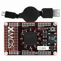
XCARD XC-1
Manufacturer Part Number
XCARD XC-1
Description
BOARD DEV KIT XS1-G4
Manufacturer
XMOS
Series
XCore™r
Type
MCUr
Datasheets
1.XS1-G04B-FB144-C4.pdf
(22 pages)
2.XCARD_XC-1.pdf
(2 pages)
3.XCARD_XC-1.pdf
(21 pages)
4.XCARD_XC-1.pdf
(17 pages)
Specifications of XCARD XC-1
Contents
Board, Cable
Lead Free Status / Rohs Status
Lead free / RoHS Compliant
For Use With/related Products
XS1-G4
Other names
880-1013


XS1-G4 144BGA Datasheet (3.5)
These signals control the PLL of the XS1-G4
2 System Services
System Services are required to support correct device behavior. These signals
control clocking, reset and boot behavior of the device.
2.1 Clock control signals
Functional description
SS_PLL_BYPASS When pin is set high, SS_CLK is used as the system clock. Set to
SS_PLL_AVDD The on-chip PLL requires a very clean AVDD power supply. It is
SS_PLL_AGND Analogue ground for the PLL. Connect directly to board ground.
SS_CLK Reference clock signal for the on-chip PLL. A default frequency of 20MHz
2.2 Miscellaneous control signals
Signal
SS_PLL_BYPASS
SS_PLL_AVDD
SS_PLL_AGND
SS_CLK
Signal
SS_XC0_BS0
SS_DEBUG
SS_RESET
SS_XC0_CFG0
SS_TEST_ENA
IO_VDD.
recommended that this supply node be separated from the other, noisier,
supplies in the board. The supply should be decoupled close to the respective
IC power pins. Nominally 1.0V.
is typically used by XS1 family devices but other frequencies can be derived
from SS_CLK using an onboard PLL. Input clock frequencies of
supported.
Ball ID
D4
E4
Ball ID
D8
E9
D5
D9
G9
I/O
I, PD
pwr
pwr
I, PD, ST
I/O
IO, PU
IO, PU, ST
I, PD, ST
I, PD
I, PD
www.xmos.com
Function Description
Control
Clock
XCore0
Function Description
Boot
status
Debug
Reset
Bypasses the PLL, using SS_CLK di-
rectly
Analog power supply to the PLL
AGND power supply for the PLL
System clock
See Boot status pins below
Activates multicore debug
Asynchronous system reset
Reserved, tie to IO_VDD
Reserved, tie pin to ground
20 MHz are
8/22
Related parts for XCARD XC-1
Image
Part Number
Description
Manufacturer
Datasheet
Request
R

Part Number:
Description:
BOARD DEV KIT XS1-G4 ETHERNET
Manufacturer:
XMOS
Datasheet:

Part Number:
Description:
BOARD DEV KIT XS1-G4
Manufacturer:
XMOS
Datasheet:

Part Number:
Description:
DEV KIT EVENT-DRIVEN PROC XS1-L1
Manufacturer:
XMOS
Datasheet:

Part Number:
Description:
BOARD KIT XS1-G4 LED CTRL TILE
Manufacturer:
XMOS
Datasheet:

Part Number:
Description:
ADAPTER USB DEBUGGER JTAG XSYS2
Manufacturer:
XMOS
Datasheet:

Part Number:
Description:
IC MPU 32BIT SINGLE CORE 64LQFP
Manufacturer:
XMOS
Datasheet:

Part Number:
Description:
IC MPU 32BIT SINGLE CORE 64LQFP
Manufacturer:
XMOS
Datasheet:
Part Number:
Description:
IC MPU 32BIT SINGLE CORE 64LQFP
Manufacturer:
XMOS
Datasheet:

Part Number:
Description:
IC MPU 32BIT SINGLE CORE 64LQFP
Manufacturer:
XMOS
Datasheet:
Part Number:
Description:
IC MPU 32BIT SINGLE CORE 64LQFP
Manufacturer:
XMOS
Datasheet:

Part Number:
Description:
IC MPU 32BIT SINGLE CORE 128TQFP
Manufacturer:
XMOS
Datasheet:
Part Number:
Description:
IC MPU 32BIT SINGLE CORE 64LQFP
Manufacturer:
XMOS
Datasheet:
Part Number:
Description:
IC MPU 32BIT SINGLE CORE 128TQFP
Manufacturer:
XMOS
Datasheet:
Part Number:
Description:
IC MPU 32BIT SINGLE CORE 128TQFP
Manufacturer:
XMOS
Datasheet:

Part Number:
Description:
IC MPU 32BIT DUAL CORE 124QFN
Manufacturer:
XMOS
Datasheet: