ADG412BNZ Analog Devices Inc, ADG412BNZ Datasheet - Page 6
ADG412BNZ
Manufacturer Part Number
ADG412BNZ
Description
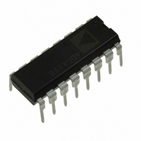
IC SWITCH QUAD SPST 16DIP
Manufacturer
Analog Devices Inc
Series
LC²MOSr
Type
Analog Switchr
Datasheet
1.ADG411BRZ.pdf
(16 pages)
Specifications of ADG412BNZ
Design Resources
Parametric Measurement Unit and Supporting Components for PAD Appls Using AD5522 and AD7685 (CN0104)
Function
Switch
Circuit
4 x SPST - NO
On-state Resistance
35 Ohm
Voltage Supply Source
Single, Dual Supply
Voltage - Supply, Single/dual (±)
12V, ±15V
Current - Supply
1µA
Operating Temperature
-40°C ~ 85°C
Mounting Type
Through Hole
Package / Case
16-DIP (0.300", 7.62mm)
Analog Switch Type
SPST
No. Of Channels
4
On State Resistance Max
35ohm
Turn Off Time
100ns
Turn On Time
110ns
Supply Voltage Range
4.5V To 5.5V
Operating Temperature Range
-40°C To +85°C
Package
16PDIP
Maximum On Resistance
80@10.8V Ohm
Maximum High Level Output Current
30 mA
Maximum Turn-off Time
100(Typ)@±15V ns
Maximum Turn-on Time
175(Typ)@12V ns
Switch Architecture
SPST
Power Supply Type
Single|Dual
Lead Free Status / RoHS Status
Lead free / RoHS Compliant


ADG411/ADG412/ADG413
PIN CONFIGURATION AND FUNCTION DESCRIPTIONS
Table 6. Pin Function Descriptions
Pin No.
1, 8, 9, 16
2, 7, 10, 15
3, 6, 11, 14
4
5
12
13
Mnemonic
IN1–IN4
D1–D4
S1–S4
V
GND
V
V
SS
L
DD
Description
Logic Control Input.
Drain Terminal. Can be an input or output.
Source Terminal. Can be an input or output.
Most Negative Power Supply Potential in Dual Supplies. In single supply applications, it may be
connected to GND.
Ground (0 V) Reference.
Logic Power Supply (5 V).
Most Positive Power Supply Potential.
GND
V
IN1
IN4
D1
S1
S4
D4
SS
Figure 4. Pin Configuration
1
2
3
4
5
6
7
8
Rev. D | Page 6 of 16
(Not to Scale)
ADG412/
ADG411/
ADG413
TOP VIEW
16
15
14
13
12
11
10
9
IN2
D2
S2
V
V
S3
D3
IN3
DD
L
Related parts for ADG412BNZ
Image
Part Number
Description
Manufacturer
Datasheet
Request
R

Part Number:
Description:
±1.7g Dual-Axis IMEMS Accelerometer Evaluation Board
Manufacturer:
Analog Devices Inc
Datasheet:

Part Number:
Description:
Inertial Sensor Evaluation System
Manufacturer:
Analog Devices Inc
Datasheet:
Part Number:
Description:
Manufacturer:
Analog Devices Inc
Datasheet:
Part Number:
Description:
Manufacturer:
Analog Devices Inc
Datasheet:
Part Number:
Description:
Manufacturer:
Analog Devices Inc
Datasheet:
Part Number:
Description:
Manufacturer:
Analog Devices Inc
Datasheet:
Part Number:
Description:
Manufacturer:
Analog Devices Inc
Datasheet:
Part Number:
Description:
Manufacturer:
Analog Devices Inc
Datasheet:
Part Number:
Description:
Manufacturer:
Analog Devices Inc
Datasheet:
Part Number:
Description:
Manufacturer:
Analog Devices Inc
Datasheet:
Part Number:
Description:
Manufacturer:
Analog Devices Inc
Datasheet:
Part Number:
Description:
Manufacturer:
Analog Devices Inc
Datasheet:
Part Number:
Description:
Manufacturer:
Analog Devices Inc
Datasheet: