ADG508FBNZ Analog Devices Inc, ADG508FBNZ Datasheet - Page 2
ADG508FBNZ
Manufacturer Part Number
ADG508FBNZ
Description
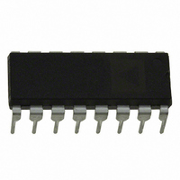
IC MULTIPLEXER 8X1 16DIP
Manufacturer
Analog Devices Inc
Type
Analog Multiplexerr
Specifications of ADG508FBNZ
Function
Multiplexer
Circuit
1 x 8:1
On-state Resistance
300 Ohm
Voltage Supply Source
Dual Supply
Voltage - Supply, Single/dual (±)
±10.8 V ~ 16.5 V
Current - Supply
20µA
Operating Temperature
-40°C ~ 85°C
Mounting Type
Through Hole
Package / Case
16-DIP (0.300", 7.62mm)
No. Of Circuits
1
Supply Current
600µA
On State Resistance Max
300ohm
Supply Voltage Range
10.8V To 16.5V
Operating Temperature Range
-40°C To +85°C
Analog Switch Case Style
DIP
Multiplexer Configuration
Single 8:1
Number Of Inputs
8
Number Of Outputs
1
Number Of Channels
1
Analog Switch On Resistance
350@±15VOhm
Analog Switch Turn On Time
250ns
Analog Switch Turn Off Time
250ns
Package Type
PDIP
Power Supply Requirement
Dual
Single Supply Voltage (min)
Not RequiredV
Single Supply Voltage (typ)
Not RequiredV
Single Supply Voltage (max)
Not RequiredV
Dual Supply Voltage (typ)
±15V
Dual Supply Voltage (max)
±22V
Power Dissipation
3.3mW
Mounting
Through Hole
Pin Count
16
Operating Temp Range
-40C to 85C
Operating Temperature Classification
Industrial
Lead Free Status / RoHS Status
Lead free / RoHS Compliant
Lead Free Status / RoHS Status
Lead free / RoHS Compliant, Lead free / RoHS Compliant


ADG508F/ADG509F/ADG528F–SPECIFICATIONS
Dual Supply
Parameter
ANALOG SWITCH
LEAKAGE CURRENTS
FAULT
DIGITAL INPUTS
DYNAMIC CHARACTERISTICS
POWER REQUIREMENTS
NOTES
1
2
Specifications subject to change without notice.
Temperature ranges are as follows: B Version: –40 C to +85 C; T Version: –55 C to +125 C.
Guaranteed by design, not subject to production test.
Analog Signal Range
R
R
R
Source OFF Leakage I
Drain OFF Leakage I
Channel ON Leakage I
Output Leakage Current
Input Leakage Current
Input Leakage Current
Input High Voltage, V
Input Low Voltage, V
Input Current
C
t
t
t
t
t
ADG528F Only
Charge Injection
OFF Isolation
C
C
I
I
TRANSITION
OPEN
ON
OFF
SETT
DD
SS
ON
ON
ON
IN
S
D
ADG508F/ADG528F
ADG509F
ADG508F/ADG528F
ADG509F
(With Overvoltage)
(With Overvoltage)
(With Power Supplies OFF)
I
0.1%
0.01%
t
t
t
t
ADG508F/ADG528F
ADG509F
W
S
H
RS
(OFF)
INL
(OFF)
, Digital Input Capacitance
(EN, WR)
, Address, Enable Setup Time
(EN, RS)
, Address, Enable Hold Time
Drift
Match
, Write Pulsewidth
, Settling Time
, Reset Pulsewidth
or I
INH
(V
DD
D
INL
= +15 V
INH
S
(OFF)
D
(OFF)
, I
S
(ON)
10%, V
2
+25 C +85 C
300
0.6
5
5
200
300
50
25
200
250
200
250
100
4
68
50
5
50
25
0.1
0.1
0.02
1
0.04
1
1
0.04
1
1
0.02
2
0.005
2
0.001
2
SS
= –15 V
B Version
–40 C to
V
V
350
400
2.4
0.8
400
10
400
400
1
2.5
120
100
10
100
0.2
0.1
50
60
30
60
30
SS
DD
2
1
+ 3
– 1.5
10%, GND = 0 V, unless otherwise noted)
+25 C +125 C
300
0.6
5
5
200
300
50
25
200
250
200
250
100
4
68
50
5
50
25
0.1
0.1
0.02
1
0.04
1
1
0.04
1
1
0.02
2
0.005
2
0.001
2
T Version
–2–
–55 C to
V
V
400
450
2.4
0.8
400
10
400
400
1
2.5
200
100
10
100
0.2
0.1
50
200
100
200
100
1
SS
DD
+ 3
– 1.5
Units
V min
V max
%/ C typ V
% max
nA typ
nA max
nA typ
nA max
nA max
nA typ
nA max
nA max
nA typ
V min
V max
pF typ
ns typ
ns max
ns typ
ns min
ns typ
ns max
ns typ
ns max
ns min
ns min
ns min
ns min
pC typ
dB typ
dB min
pF typ
pF typ
pF typ
mA max
mA max
A max
A typ
A max
A typ
A max
A max
s typ
s typ
typ
max
Test Conditions/Comments
–10 V < V
V
–10 V < V
V
V
V
Test Circuit 2
V
Test Circuit 3
V
Test Circuit 4
V
V
V
Test Circuit 6
V
R
V
R
V
R
V
R
V
R
V
V
R
V
V
DD
DD
S
S
D
D
S
S
S
S
IN
S1
S
S
S
S
S
S
IN
L
L
L
L
L
L
= 0 V, R
= 0 V, I
= 0 V, I
= V
= 33 V, V
= 25 V, V
= 25 V, V
= +5 V; Test Circuit 8
= +5 V; Test Circuit 9
= +5 V; Test Circuit 9
= +5 V
= 7 V rms; Test Circuit 13
= 1 M , C
= 1 k , C
= 1 k , C
= 1 k , C
= 1 k , C
= 1 k , C
1
= 10 V, V
= 10 V, V
= 10 V, V
= 0 or V
= 0 V or 5 V
= +15 V
= +15 V
D
= 10 V;
S
S
S
S
S
< +10 V, I
< +10 V, I
= 1 mA
= 1 mA
DD
= 0 , C
L
L
L
L
L
D
D
D
L
S
S
= 35 pF;
= 35 pF;
= 35 pF;
= 35 pF;
= 15 pF, f = 100 kHz;
S8
10%, V
5%, V
= 35 pF;
= 10 V;
= 10 V;
= 0 V, Test Circuit 3
=
= V
=
EN
10 V, Test Circuit 5
L
10 V; Test Circuit 7
= 1 nF; Test Circuit 12
SS
S
S
= A0, A1, A2 = 0 V
SS
= 1 mA;
= 1 mA;
= –15 V
= –15 V
5%
REV. C
10%
Related parts for ADG508FBNZ
Image
Part Number
Description
Manufacturer
Datasheet
Request
R

Part Number:
Description:
±1.7g Dual-Axis IMEMS Accelerometer Evaluation Board
Manufacturer:
Analog Devices Inc
Datasheet:

Part Number:
Description:
Inertial Sensor Evaluation System
Manufacturer:
Analog Devices Inc
Datasheet:
Part Number:
Description:
Manufacturer:
Analog Devices Inc
Datasheet:
Part Number:
Description:
Manufacturer:
Analog Devices Inc
Datasheet:
Part Number:
Description:
Manufacturer:
Analog Devices Inc
Datasheet:
Part Number:
Description:
Manufacturer:
Analog Devices Inc
Datasheet:
Part Number:
Description:
Manufacturer:
Analog Devices Inc
Datasheet:
Part Number:
Description:
Manufacturer:
Analog Devices Inc
Datasheet:
Part Number:
Description:
Manufacturer:
Analog Devices Inc
Datasheet:
Part Number:
Description:
Manufacturer:
Analog Devices Inc
Datasheet:
Part Number:
Description:
Manufacturer:
Analog Devices Inc
Datasheet:
Part Number:
Description:
Manufacturer:
Analog Devices Inc
Datasheet:
Part Number:
Description:
Manufacturer:
Analog Devices Inc
Datasheet: