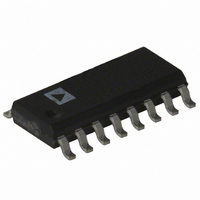
ADG438FBRZ Analog Devices Inc, ADG438FBRZ Datasheet - Page 4

ADG438FBRZ
Manufacturer Part Number
ADG438FBRZ
Description
IC MULTIPLEXER 8X1 16SOIC
Manufacturer
Analog Devices Inc
Specifications of ADG438FBRZ
Function
Multiplexer
Circuit
1 x 8:1
On-state Resistance
400 Ohm
Current - Supply
0.05mA
Operating Temperature
-40°C ~ 85°C
Mounting Type
Surface Mount
Package / Case
16-SOIC (0.154", 3.90mm Width)
No. Of Circuits
1
Supply Current
250nA
On State Resistance Max
400ohm
Supply Voltage Range
± 15V
Operating Temperature Range
-40°C To +105°C
Analog Switch Case Style
SOIC
No. Of Pins
16
Lead Free Status / RoHS Status
Lead free / RoHS Compliant
Available stocks
Company
Part Number
Manufacturer
Quantity
Price
Part Number:
ADG438FBRZ
Manufacturer:
ADI/亚德诺
Quantity:
20 000
ADG438F/ADG439F
TERMINOLOGY
V
V
GND
R
R
R
I
I
I
V
C
C
C
C
t
t
t
t
V
V
I
Off Isolation
Charge Injection
I
I
ON
OFF
TRANSITION
OPEN
S
D
D
INL
DD
SS
R
DD
SS
ON
ON
ON
D
INL
INH
S
D
D
IN
(OFF)
, I
(OFF)
ON
, C
(OFF)
(V
(OFF)
(EN)
S
(EN)
(I
Drift
Match
(ON)
S
S
INH
)
(ON)
)
Most positive power supply potential.
Most negative power supply potential.
Ground (0 V) reference.
Ohmic resistance between D and S.
R
input voltage with a constant load current.
Change in R
by one degree Celsius.
Difference between the R
channels.
Source leakage current when the switch is
off.
Drain leakage current when the switch is off.
Channel leakage current when the switch is
on.
Analog voltage on terminals D, S.
Channel input capacitance for “OFF”
condition.
Channel output capacitance for “OFF”
condition.
“ON” switch capacitance.
Digital input capacitance.
Delay time between the 50% and 90% points
of the digital input and switch “ON”
condition.
Delay time between the 50% and 90% points
of the digital input and switch “OFF”
condition.
Delay time between the 50% and 90% points
of the digital inputs and the switch “ON”
condition when switching from one address
state to another.
“OFF” time measured between 80% points of
both switches when switching from one
address state to another.
Maximum input voltage for Logic “0”.
Minimum input voltage for Logic “1”.
Input current of the digital input.
A measure of unwanted signal coupling
through an “OFF” channel.
A measure of the glitch impulse transferred
from the digital input to the analog output
during switching.
Positive supply current.
Negative supply current.
ON
variation due to a change in the analog
ON
when temperature changes
ON
of any two
–4–
Typical Performance Graphs
Figure 2. Input Leakage Current as a Function of V
(Power Supplies OFF) During Overvoltage Conditions
Figure 3. Output Leakage Current as a Function of V
(Power Supplies ON) During Overvoltage Conditions
Figure 1. On Resistance as a Function of V
100
100
2000
1750
1500
1250
1000
100n
100p
100n
100p
10
10
750
500
250
10n
10p
10n
10p
1m
1m
1
1
1n
1p
1n
1p
0
–15
–50
–50
–40
–40
–10
–30
–30
–20
–20
V
V
IN
IN
–5
– INPUT VOLTAGE – Volts
– INPUT VOLTAGE – Volts
–10
–10
OPERATING RANGE
OPERATING RANGE
V
V
V
D
DD
SS
T
V
V
A
(V
0
0
DD
SS
= –10V
= +10V
= +25 C
S
0
) – Volts
= –5V
= +5V
10
10
20
20
5
30
30
V
V
V
DD
SS
D
V
V
V
= 0V
V
V
40
= –15V
40
DD
SS
D
= +15V
10
DD
SS
= 0V
= 0V
= 0V
= –15V
= +15V
50
50
D
(V
15
60
60
REV. D
S
)
S
S


